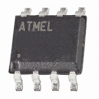
ATTINY25V-15ST Atmel, ATTINY25V-15ST Datasheet - Page 127

ATTINY25V-15ST
Manufacturer Part Number
ATTINY25V-15ST
Description
MCU AVR 2K FLASH 4MHZ 8-SOIC
Manufacturer
Atmel
Series
AVR® ATtinyr
Datasheet
1.ATTINY25-15MZ.pdf
(196 pages)
Specifications of ATTINY25V-15ST
Package / Case
8-SOIC (3.9mm Width)
Voltage - Supply (vcc/vdd)
1.8 V ~ 3.6 V
Operating Temperature
-40°C ~ 85°C
Speed
8MHz
Number Of I /o
6
Eeprom Size
128 x 8
Core Processor
AVR
Program Memory Type
FLASH
Ram Size
128 x 8
Program Memory Size
2KB (2K x 8)
Data Converters
A/D 4x10b
Oscillator Type
Internal
Peripherals
Brown-out Detect/Reset, POR, PWM, WDT
Connectivity
USI
Core Size
8-Bit
Processor Series
ATTINY2x
Core
AVR8
Data Bus Width
8 bit
Data Ram Size
128 B
Maximum Operating Temperature
+ 85 C
Mounting Style
SMD/SMT
Lead Free Status / RoHS Status
Lead free / RoHS Compliant
Available stocks
Company
Part Number
Manufacturer
Quantity
Price
Part Number:
ATTINY25V-15ST
Manufacturer:
ATMEL/爱特梅尔
Quantity:
20 000
- Current page: 127 of 196
- Download datasheet (4Mb)
18.7.9
7598H–AVR–07/09
Digital Input Disable Register 0 – DIDR0
• Bit 5 – IPR: Input Polarity Mode
The Input Polarity mode allows software selectable differential input pairs and full 10 bit ADC
resolution, in the unipolar input mode, assuming a pre-determined input polarity. If the input
polarity is not known it is actually possible to determine the polarity first by using the bipolar input
mode (with 9 bit resolution + 1 sign bit ADC measurement). And once determined, set or clear
the polarity reversal bit, as needed, for a succeeding 10 bit unipolar measurement.
• Bits 4..3 – Res: Reserved Bits
These bits are reserved bits in the ATtiny25/45/85 and will always read as zero.
• Bits 2:0 – ADTS2:0: ADC Auto Trigger Source
If ADATE in ADCSRA is written to one, the value of these bits selects which source will trigger
an ADC conversion. If ADATE is cleared, the ADTS2:0 settings will have no effect. A conversion
will be triggered by the rising edge of the selected Interrupt Flag. Note that switching from a trig-
ger source that is cleared to a trigger source that is set, will generate a positive edge on the
trigger signal. If ADEN in ADCSRA is set, this will start a conversion. Switching to Free Running
mode (ADTS[2:0]=0) will not cause a trigger event, even if the ADC Interrupt Flag is set.
Table 18-6.
• Bits 5..2 – ADC3D..ADC0D: ADC3..0 Digital Input Disable
When this bit is written logic one, the digital input buffer on the corresponding ADC pin is dis-
abled. The corresponding PIN register bit will always read as zero when this bit is set. When an
analog signal is applied to the ADC3..0 pin and the digital input from this pin is not needed, this
bit should be written logic one to reduce power consumption in the digital input buffer.
Bit
Read/Write
Initial Value
ADTS2
0
0
0
0
1
1
1
ADC Auto Trigger Source Selections
R
7
–
0
ADTS1
R
6
–
0
0
0
1
1
0
0
1
ADC0D
R/W
5
0
ADC2D
R/W
ADTS0
4
0
0
1
0
1
0
1
0
ADC3D
R/W
3
0
Trigger Source
Free Running mode
Analog Comparator
External Interrupt Request 0
Timer/Counter Compare Match A
Timer/Counter Overflow
Timer/Counter Compare Match B
Pin Change Interrupt Request
ADC1D
R/W
2
0
ATtiny25/45/85
AIN1D
R/W
1
0
AIN0D
R/W
0
0
DIDR0
127
Related parts for ATTINY25V-15ST
Image
Part Number
Description
Manufacturer
Datasheet
Request
R

Part Number:
Description:
IC MCU AVR 2K FLASH 10MHZ 20-QFN
Manufacturer:
Atmel
Datasheet:

Part Number:
Description:
MCU AVR 2KB FLASH 10MHZ 8SOIC
Manufacturer:
Atmel
Datasheet:

Part Number:
Description:
IC AVR MCU 2K 10MHZ 8-DIP
Manufacturer:
Atmel
Datasheet:

Part Number:
Description:
IC MCU AVR 2KB FLASH 10MHZ 8SOIC
Manufacturer:
Atmel
Datasheet:

Part Number:
Description:
IC MCU AVR 2KB FLASH 10MHZ 8SOIC
Manufacturer:
Atmel
Datasheet:

Part Number:
Description:
MCU AVR 2KB FLASH 10MHZ 8SOIC
Manufacturer:
Atmel
Datasheet:

Part Number:
Description:
MCU AVR 2KB FLASH 10MHZ 20QFN
Manufacturer:
Atmel
Datasheet:

Part Number:
Description:
MCU AVR 2K ISP FLASH 1.8V 8-SOIC
Manufacturer:
Atmel
Datasheet:

Part Number:
Description:
IC AVR MCU 2K 10MHZ 8DIP
Manufacturer:
Atmel
Datasheet:

Part Number:
Description:
IC AVR MCU 2K 10MHZ 8SOIC
Manufacturer:
Atmel
Datasheet:

Part Number:
Description:
8-bit Microcontrollers - MCU 2KB FLASH,128B EE, 128B SRAM-10MHz
Manufacturer:
Atmel

Part Number:
Description:
8-bit Microcontrollers - MCU 2KB FL,128B EE,128B SRAM-10MHz
Manufacturer:
Atmel

Part Number:
Description:
8-bit Microcontrollers - MCU AVR 16KB FL 512B EE 1KB SRAM 10 MHZ GRN
Manufacturer:
Atmel


