ATTINY44-15MZ Atmel, ATTINY44-15MZ Datasheet - Page 130
ATTINY44-15MZ
Manufacturer Part Number
ATTINY44-15MZ
Description
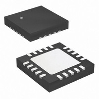
MCU AVR 4K FLASH 15MHZ 20-QFN
Manufacturer
Atmel
Series
AVR® ATtinyr
Datasheet
1.ATTINY44-15MZ.pdf
(225 pages)
Specifications of ATTINY44-15MZ
Package / Case
20-QFN Exposed Pad
Voltage - Supply (vcc/vdd)
2.7 V ~ 5.5 V
Operating Temperature
-40°C ~ 125°C
Speed
16MHz
Number Of I /o
12
Eeprom Size
256 x 8
Core Processor
AVR
Program Memory Type
FLASH
Ram Size
256 x 8
Program Memory Size
4KB (4K x 8)
Data Converters
A/D 8x10b
Oscillator Type
Internal
Peripherals
Brown-out Detect/Reset, POR, PWM, WDT
Connectivity
USI
Core Size
8-Bit
Processor Series
ATTINY4x
Core
AVR8
Data Bus Width
8 bit
Data Ram Size
256 B
Interface Type
SPI, UART
Maximum Clock Frequency
16 MHz
Number Of Programmable I/os
12
Number Of Timers
2
Maximum Operating Temperature
+ 85 C
Mounting Style
SMD/SMT
3rd Party Development Tools
EWAVR, EWAVR-BL
Development Tools By Supplier
ATAVRDRAGON, ATSTK500, ATSTK600, ATAVRISP2, ATAVRONEKIT
Minimum Operating Temperature
- 40 C
On-chip Adc
10 bit, 8 Channel
Lead Free Status / RoHS Status
Lead free / RoHS Compliant
Available stocks
Company
Part Number
Manufacturer
Quantity
Price
Company:

Part Number:
ATTINY44-15MZ
Manufacturer:
ATMEL
Quantity:
1 000
Part Number:
ATTINY44-15MZ
Manufacturer:
ATMEL/爱特梅尔
Quantity:
20 000


16.5
16.5.1
16.5.2
16.5.3
130
Register Descriptions
Atmel ATtiny24/44/84 [Preliminary]
USIBR – USI Data Buffer
USIDR – USI Data Register
USISR – USI Status Register
The USI uses no buffering for the serial register, i.e., when accessing the data register
(USIDR) the serial register is accessed directly. If a serial clock occurs during the same cycle
the register is written, the register will contain the value written and no shift is performed. A
(left) shift operation is performed depending on the USICS1..0 bit settings. The shift operation
can be controlled by an external clock edge, by a timer/counter 0 compare match, or directly
by software using the USICLK strobe bit. Note that even when no wire mode is selected
(USIWM1..0 = 0), both the external data input (DI/SDA) and the external clock input
(USCK/SCL) can still be used by the shift register.
The output pin in use - DO or SDA, depending on the wire mode - is connected via the output
latch to the most-significant bit (bit 7) of the data register. The output latch is open (transpar-
ent) during the first half of a serial clock cycle when an external clock source is selected
(USICS1 = 1), and constantly open when an internal clock source is used (USICS1 = 0). The
output will be changed immediately when a new MSB is written as long as the latch is open.
The latch ensures that data input is sampled and data output is changed on opposite clock
edges.
Note that the corresponding Data Direction Register to the pin must be set to one for enabling
data output from the Shift Register.
The Status Register contains Interrupt Flags, line Status Flags and the counter value.
• Bit 7 – USISIF: Start Condition Interrupt Flag
When two-wire mode is selected, the USISIF flag is set (one) when a start condition is
detected. When output disable mode or three-wire mode is selected and (USICSx = 0b11 and
USICLK = 0) or (USICS = 0b10 and USICLK = 0), any edge on the SCK pin sets the flag.
Bit
0x10 (0x30)
Read/Write
Initial Value
Bit
0x0F (0x2F)
Read/Write
Initial Value
Bit
0x0E (0x2E)
Read/Write
Initial Value
USISIF
R/W
MSB
MSB
R/W
7
0
R
7
0
7
0
USIOIF
R/W
6
0
R/W
R
6
0
6
0
USIPF
R/W
5
0
R/W
R
0
0
5
5
USIDC
4
R
0
R/W
R
4
0
4
0
USICNT3
R/W
3
0
R/W
R
3
0
3
0
USICNT2
R/W
2
0
R/W
R
2
0
2
0
USICNT1
R/W
R/W
1
0
R
1
0
1
0
USICNT0
LSB
LSB
R/W
R/W
R
0
0
0
0
0
0
7701E–AVR–02/11
USIBR
USIDR
USISR
Related parts for ATTINY44-15MZ
Image
Part Number
Description
Manufacturer
Datasheet
Request
R

Part Number:
Description:
Manufacturer:
Atmel Corporation
Datasheet:
Part Number:
Description:
Manufacturer:
Atmel Corporation
Datasheet:

Part Number:
Description:
IC MCU AVR 4K FLASH 20MHZ 20-QFN
Manufacturer:
Atmel
Datasheet:

Part Number:
Description:
IC MCU AVR 4K FLASH 20MHZ 14SOIC
Manufacturer:
Atmel
Datasheet:

Part Number:
Description:
MCU AVR 4KB FLASH 20MHZ 14SOIC
Manufacturer:
Atmel
Datasheet:
Part Number:
Description:
MCU AVR 4KB FLASH 20MHZ 20QFN
Manufacturer:
Atmel
Datasheet:
Part Number:
Description:
IC MCU AVR 4K FLASH 15MHZ 14SOIC
Manufacturer:
Atmel
Datasheet:

Part Number:
Description:
IC MCU AVR 4K FLASH 20MHZ 14-DIP
Manufacturer:
Atmel
Datasheet:
Part Number:
Description:
Manufacturer:
Atmel Corporation
Datasheet:
Part Number:
Description:
Microcontrollers (MCU) 512B FL 32B SRAM TIMER ATTINY4 12MHz
Manufacturer:
Atmel
Part Number:
Description:
IC MCU AVR 512B FLASH SOT-23-6
Manufacturer:
Atmel
Datasheet:

Part Number:
Description:
IC MCU AVR 512B FLASH SOT-23-6
Manufacturer:
Atmel
Datasheet: