ATTINY44-15MZ Atmel, ATTINY44-15MZ Datasheet - Page 167
ATTINY44-15MZ
Manufacturer Part Number
ATTINY44-15MZ
Description
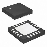
MCU AVR 4K FLASH 15MHZ 20-QFN
Manufacturer
Atmel
Series
AVR® ATtinyr
Datasheet
1.ATTINY44-15MZ.pdf
(225 pages)
Specifications of ATTINY44-15MZ
Package / Case
20-QFN Exposed Pad
Voltage - Supply (vcc/vdd)
2.7 V ~ 5.5 V
Operating Temperature
-40°C ~ 125°C
Speed
16MHz
Number Of I /o
12
Eeprom Size
256 x 8
Core Processor
AVR
Program Memory Type
FLASH
Ram Size
256 x 8
Program Memory Size
4KB (4K x 8)
Data Converters
A/D 8x10b
Oscillator Type
Internal
Peripherals
Brown-out Detect/Reset, POR, PWM, WDT
Connectivity
USI
Core Size
8-Bit
Processor Series
ATTINY4x
Core
AVR8
Data Bus Width
8 bit
Data Ram Size
256 B
Interface Type
SPI, UART
Maximum Clock Frequency
16 MHz
Number Of Programmable I/os
12
Number Of Timers
2
Maximum Operating Temperature
+ 85 C
Mounting Style
SMD/SMT
3rd Party Development Tools
EWAVR, EWAVR-BL
Development Tools By Supplier
ATAVRDRAGON, ATSTK500, ATSTK600, ATAVRISP2, ATAVRONEKIT
Minimum Operating Temperature
- 40 C
On-chip Adc
10 bit, 8 Channel
Lead Free Status / RoHS Status
Lead free / RoHS Compliant
Available stocks
Company
Part Number
Manufacturer
Quantity
Price
Company:

Part Number:
ATTINY44-15MZ
Manufacturer:
ATMEL
Quantity:
1 000
Part Number:
ATTINY44-15MZ
Manufacturer:
ATMEL/爱特梅尔
Quantity:
20 000


21.6
7701E–AVR–02/11
Serial Downloading
Both the Flash and EEPROM memory arrays can be programmed using the serial SPI bus
while RESET is pulled to GND. The serial interface consists of pins SCK, MOSI (input) and
MISO (output). After RESET is set low, the Programming Enable instruction needs to be exe-
cuted first before program/erase operations can be executed. NOTE, in
167, the pin mapping for SPI programming is listed. Not all parts use the SPI pins dedicated
for the internal SPI interface.
Figure 21-1. Serial Programming and Verify
Note:
Table 21-9.
When programming the EEPROM, an auto-erase cycle is built into the self-timed program-
ming operation (in serial mode only), and there is no need to first execute the chip erase
instruction. The chip erase operation turns the content of every memory location in both the
program and EEPROM arrays into 0xFF.
Depending on the CKSEL fuses, a valid clock must be present. The minimum low and high
periods for the serial clock (SCK) input are defined as follows:
Low: > 2 CPU clock cycles for f
High: > 2 CPU clock cycles for f
1. If the device is clocked by the internal oscillator, it is not needed to connect a clock source to
Symbol
MOSI
MISO
SCK
the CLKI pin.
Pin Mapping Serial Programming
Atmel ATtiny24/44/84 [Preliminary]
MOSI
MISO
SCK
ck
ck
Pins
PA6
PA5
PA4
< 12MHz, 3 CPU clock cycles for f
< 12MHz, 3 CPU clock cycles for f
RESET
GND
(1)
VCC
I/O
O
I
I
+1.8 - 5.5V
ck
ck
>= 12MHz
>= 12MHz
Description
Serial Data in
Serial Data out
Serial Clock
Table 21-9 on page
167
Related parts for ATTINY44-15MZ
Image
Part Number
Description
Manufacturer
Datasheet
Request
R

Part Number:
Description:
Manufacturer:
Atmel Corporation
Datasheet:
Part Number:
Description:
Manufacturer:
Atmel Corporation
Datasheet:

Part Number:
Description:
IC MCU AVR 4K FLASH 20MHZ 20-QFN
Manufacturer:
Atmel
Datasheet:

Part Number:
Description:
IC MCU AVR 4K FLASH 20MHZ 14SOIC
Manufacturer:
Atmel
Datasheet:

Part Number:
Description:
MCU AVR 4KB FLASH 20MHZ 14SOIC
Manufacturer:
Atmel
Datasheet:
Part Number:
Description:
MCU AVR 4KB FLASH 20MHZ 20QFN
Manufacturer:
Atmel
Datasheet:
Part Number:
Description:
IC MCU AVR 4K FLASH 15MHZ 14SOIC
Manufacturer:
Atmel
Datasheet:

Part Number:
Description:
IC MCU AVR 4K FLASH 20MHZ 14-DIP
Manufacturer:
Atmel
Datasheet:
Part Number:
Description:
Manufacturer:
Atmel Corporation
Datasheet:
Part Number:
Description:
Microcontrollers (MCU) 512B FL 32B SRAM TIMER ATTINY4 12MHz
Manufacturer:
Atmel
Part Number:
Description:
IC MCU AVR 512B FLASH SOT-23-6
Manufacturer:
Atmel
Datasheet:

Part Number:
Description:
IC MCU AVR 512B FLASH SOT-23-6
Manufacturer:
Atmel
Datasheet: