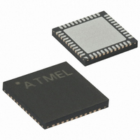
ATMEGA8515-16MU Atmel, ATMEGA8515-16MU Datasheet - Page 104

ATMEGA8515-16MU
Manufacturer Part Number
ATMEGA8515-16MU
Description
IC AVR MCU 8K 16MHZ 5V 44-QFN
Manufacturer
Atmel
Series
AVR® ATmegar
Specifications of ATMEGA8515-16MU
Core Processor
AVR
Core Size
8-Bit
Speed
16MHz
Connectivity
EBI/EMI, SPI, UART/USART
Peripherals
Brown-out Detect/Reset, POR, PWM, WDT
Number Of I /o
35
Program Memory Size
8KB (4K x 16)
Program Memory Type
FLASH
Eeprom Size
512 x 8
Ram Size
512 x 8
Voltage - Supply (vcc/vdd)
4.5 V ~ 5.5 V
Oscillator Type
Internal
Operating Temperature
-40°C ~ 85°C
Package / Case
44-VQFN Exposed Pad
Processor Series
ATMEGA8x
Core
AVR8
Data Bus Width
8 bit
Data Ram Size
512 B
Interface Type
SPI, USART
Maximum Clock Frequency
16 MHz
Number Of Programmable I/os
35
Number Of Timers
2
Operating Supply Voltage
4.5 V to 5.5 V
Maximum Operating Temperature
+ 85 C
Mounting Style
SMD/SMT
3rd Party Development Tools
EWAVR, EWAVR-BL
Development Tools By Supplier
ATAVRDRAGON, ATSTK500, ATSTK600, ATAVRISP2, ATAVRONEKIT
Minimum Operating Temperature
- 40 C
For Use With
ATAVRISP2 - PROGRAMMER AVR IN SYSTEMATSTK500 - PROGRAMMER AVR STARTER KIT
Lead Free Status / RoHS Status
Lead free / RoHS Compliant
Data Converters
-
Lead Free Status / Rohs Status
Details
- Current page: 104 of 257
- Download datasheet (2Mb)
Input Capture Unit
104
ATmega8515(L)
how waveforms are generated on the Output Compare outputs OC1x. For more details
about advanced counting sequences and waveform generation, see “Modes of Opera-
tion” on page 109.
The Timer/Counter Overflow (TOV1) Flag is set according to the mode of operation
selected by the WGM13:0 bits. TOV1 can be used for generating a CPU interrupt.
The Timer/Counter incorporates an Input Capture unit that can capture external events
and give them a time-stamp indicating time of occurrence. The external signal indicating
an event, or multiple events, can be applied via the ICP1 pin or alternatively, via the
Analog Comparator unit. The time-stamps can then be used to calculate frequency,
duty-cycle, and other features of the signal applied. Alternatively the time-stamps can be
used for creating a log of the events.
The Input Capture unit is illustrated by the block diagram shown in Figure 49. The ele-
ments of the block diagram that are not directly a part of the Input Capture unit are gray
shaded. The small “n” in register and bit names indicates the Timer/Counter number.
Figure 49. Input Capture Unit Block Diagram
When a change of the logic level (an event) occurs on the Input Capture pin (ICP1),
alternatively on the Analog Comparator output (ACO), and this change confirms to the
setting of the edge detector, a capture will be triggered. When a capture is triggered, the
16-bit value of the counter (TCNT1) is written to the Input Capture Register (ICR1). The
Input Capture Flag (ICF1) is set at the same system clock as the TCNT1 value is copied
into ICR1 Register. If enabled (TICIE1 = 1), the Input Capture Flag generates an Input
Capture interrupt. The ICF1 Flag is automatically cleared when the interrupt is executed.
Alternatively the ICF1 Flag can be cleared by software by writing a logical one to its I/O
bit location.
Reading the 16-bit value in the Input Capture Register (ICR1) is done by first reading the
low byte (ICR1L) and then the high byte (ICR1H). When the low byte is read the high
ICPn
WRITE
ICRnH (8-bit)
TEMP (8-bit)
Comparator
Analog
ICRn (16-bit Register)
ACO*
ICRnL (8-bit)
ACIC*
DATA BUS
Canceler
Noise
ICNC
(8-bit)
TCNTnH (8-bit)
TCNTn (16-bit Counter)
Detector
ICES
Edge
TCNTnL (8-bit)
2512K–AVR–01/10
ICFn (Int.Req.)
Related parts for ATMEGA8515-16MU
Image
Part Number
Description
Manufacturer
Datasheet
Request
R

Part Number:
Description:
IC AVR MCU 2.4GHZ XCEIVER 64QFN
Manufacturer:
Atmel
Datasheet:

Part Number:
Description:
Manufacturer:
Atmel
Datasheet:

Part Number:
Description:
MCU ATMEGA644/AT86RF230 40-DIP
Manufacturer:
Atmel
Datasheet:

Part Number:
Description:
BUNDLE ATMEGA644P/AT86RF230 QFN
Manufacturer:
Atmel
Datasheet:

Part Number:
Description:
BUNDLE ATMEGA644P/AT86RF230 TQFP
Manufacturer:
Atmel
Datasheet:

Part Number:
Description:
MCU ATMEGA1281/AT86RF230 64-TQFP
Manufacturer:
Atmel
Datasheet:

Part Number:
Description:
MCU ATMEGA1280/AT86RF230 100TQFP
Manufacturer:
Atmel
Datasheet:

Part Number:
Description:
BUNDLE ATMEGA1280/AT86RF100-TQFP
Manufacturer:
Atmel
Datasheet:

Part Number:
Description:
BUNDLE ATMEGA2560V/AT86RF230-ZU
Manufacturer:
Atmel
Datasheet:

Part Number:
Description:
MCU ATMEGA2561/AT86RF230 64-TQFP
Manufacturer:
Atmel
Datasheet:

Part Number:
Description:
INTERVAL AND WIPE/WASH WIPER CONTROL IC WITH DELAY
Manufacturer:
ATMEL Corporation
Datasheet:

Part Number:
Description:
Low-Voltage Voice-Switched IC for Hands-Free Operation
Manufacturer:
ATMEL Corporation
Datasheet:

Part Number:
Description:
MONOLITHIC INTEGRATED FEATUREPHONE CIRCUIT
Manufacturer:
ATMEL Corporation
Datasheet:

Part Number:
Description:
AM-FM Receiver IC U4255BM-M
Manufacturer:
ATMEL Corporation
Datasheet:


