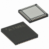
ATMEGA8515-16MU Atmel, ATMEGA8515-16MU Datasheet - Page 119

ATMEGA8515-16MU
Manufacturer Part Number
ATMEGA8515-16MU
Description
IC AVR MCU 8K 16MHZ 5V 44-QFN
Manufacturer
Atmel
Series
AVR® ATmegar
Specifications of ATMEGA8515-16MU
Core Processor
AVR
Core Size
8-Bit
Speed
16MHz
Connectivity
EBI/EMI, SPI, UART/USART
Peripherals
Brown-out Detect/Reset, POR, PWM, WDT
Number Of I /o
35
Program Memory Size
8KB (4K x 16)
Program Memory Type
FLASH
Eeprom Size
512 x 8
Ram Size
512 x 8
Voltage - Supply (vcc/vdd)
4.5 V ~ 5.5 V
Oscillator Type
Internal
Operating Temperature
-40°C ~ 85°C
Package / Case
44-VQFN Exposed Pad
Processor Series
ATMEGA8x
Core
AVR8
Data Bus Width
8 bit
Data Ram Size
512 B
Interface Type
SPI, USART
Maximum Clock Frequency
16 MHz
Number Of Programmable I/os
35
Number Of Timers
2
Operating Supply Voltage
4.5 V to 5.5 V
Maximum Operating Temperature
+ 85 C
Mounting Style
SMD/SMT
3rd Party Development Tools
EWAVR, EWAVR-BL
Development Tools By Supplier
ATAVRDRAGON, ATSTK500, ATSTK600, ATAVRISP2, ATAVRONEKIT
Minimum Operating Temperature
- 40 C
For Use With
ATAVRISP2 - PROGRAMMER AVR IN SYSTEMATSTK500 - PROGRAMMER AVR STARTER KIT
Lead Free Status / RoHS Status
Lead free / RoHS Compliant
Data Converters
-
Lead Free Status / Rohs Status
Details
- Current page: 119 of 257
- Download datasheet (2Mb)
16-bit Timer/Counter
Register Description
Timer/Counter1 Control
Register A – TCCR1A
2512K–AVR–01/10
• Bit 7:6 – COM1A1:0: Compare Output Mode for Channel A
• Bit 5:4 – COM1B1:0: Compare Output Mode for Channel B
The COM1A1:0 and COM1B1:0 control the Output Compare pins (OC1A and OC1B
respectively) behavior. If one or both of the COM1A1:0 bits are written to one, the OC1A
output overrides the normal port functionality of the I/O pin it is connected to. If one or
both of the COM1B1:0 bit are written to one, the OC1B output overrides the normal port
functionality of the I/O pin it is connected to. However, note that the Data Direction Reg-
ister (DDR) bit corresponding to the OC1A or OC1B pin must be set in order to enable
the output driver.
When the OC1A or OC1B is connected to the pin, the function of the COM1x1:0 bits is
dependent of the WGM13:0 bits setting. Table 50 shows the COM1x1:0 bit functionality
when the WGM13:0 bits are set to a normal or a CTC mode (non-PWM).
Table 50. Compare Output Mode, non-PWM
Table 51 shows the COM1x1:0 bit functionality when the WGM13:0 bits are set to the
fast PWM mode.
Table 51. Compare Output Mode, Fast PWM
Note:
Table 52 shows the COM1x1:0 bit functionality when the WGM13:0 bits are set to the
phase correct or the phase and frequency correct, PWM mode.
Bit
Read/Write
Initial Value
COM1A1/
COM1A1/
COM1B1
COM1B1
0
0
1
1
0
0
1
1
1. A special case occurs when OCR1A/OCR1B equals TOP and COM1A1/COM1B1 is
set. In this case the Compare Match is ignored, but the set or clear is done at TOP.
See “Fast PWM Mode” on page 111. for more details.
COM1A1
R/W
COM1A0/
7
0
COM1B0
COM1A0/
COM1B0
0
1
0
1
0
1
0
1
COM1A0
R/W
6
0
Description
Normal port operation, OC1A/OC1B disconnected.
WGM13:0 = 15: Toggle OC1A on Compare Match, OC1B
disconnected (Normal port operation). For all other WGM1
setting, Normal port operation, OC1A/OC1B disconnected.
Clear OC1A/OC1B on Compare Match, set OC1A/OC1B at TOP
(Non-Inverting).
Set OC1A/OC1B on Compare Match, clear OC1A/OC1B at TOP
(Inverting).
Description
Normal port operation, OC1A/OC1B disconnected.
Toggle OC1A/OC1B on Compare Match.
Clear OC1A/OC1B on Compare Match (Set output to low level).
Set OC1A/OC1B on Compare Match (Set output to high level).
COM1B1
R/W
5
0
COM1B0
R/W
4
0
(1)
FOC1A
W
3
0
FOC1B
ATmega8515(L)
W
2
0
WGM11
R/W
1
0
WGM10
R/W
0
0
TCCR1A
119
Related parts for ATMEGA8515-16MU
Image
Part Number
Description
Manufacturer
Datasheet
Request
R

Part Number:
Description:
IC AVR MCU 2.4GHZ XCEIVER 64QFN
Manufacturer:
Atmel
Datasheet:

Part Number:
Description:
Manufacturer:
Atmel
Datasheet:

Part Number:
Description:
MCU ATMEGA644/AT86RF230 40-DIP
Manufacturer:
Atmel
Datasheet:

Part Number:
Description:
BUNDLE ATMEGA644P/AT86RF230 QFN
Manufacturer:
Atmel
Datasheet:

Part Number:
Description:
BUNDLE ATMEGA644P/AT86RF230 TQFP
Manufacturer:
Atmel
Datasheet:

Part Number:
Description:
MCU ATMEGA1281/AT86RF230 64-TQFP
Manufacturer:
Atmel
Datasheet:

Part Number:
Description:
MCU ATMEGA1280/AT86RF230 100TQFP
Manufacturer:
Atmel
Datasheet:

Part Number:
Description:
BUNDLE ATMEGA1280/AT86RF100-TQFP
Manufacturer:
Atmel
Datasheet:

Part Number:
Description:
BUNDLE ATMEGA2560V/AT86RF230-ZU
Manufacturer:
Atmel
Datasheet:

Part Number:
Description:
MCU ATMEGA2561/AT86RF230 64-TQFP
Manufacturer:
Atmel
Datasheet:

Part Number:
Description:
INTERVAL AND WIPE/WASH WIPER CONTROL IC WITH DELAY
Manufacturer:
ATMEL Corporation
Datasheet:

Part Number:
Description:
Low-Voltage Voice-Switched IC for Hands-Free Operation
Manufacturer:
ATMEL Corporation
Datasheet:

Part Number:
Description:
MONOLITHIC INTEGRATED FEATUREPHONE CIRCUIT
Manufacturer:
ATMEL Corporation
Datasheet:

Part Number:
Description:
AM-FM Receiver IC U4255BM-M
Manufacturer:
ATMEL Corporation
Datasheet:


