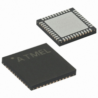
ATMEGA8515-16MU Atmel, ATMEGA8515-16MU Datasheet - Page 126

ATMEGA8515-16MU
Manufacturer Part Number
ATMEGA8515-16MU
Description
IC AVR MCU 8K 16MHZ 5V 44-QFN
Manufacturer
Atmel
Series
AVR® ATmegar
Specifications of ATMEGA8515-16MU
Core Processor
AVR
Core Size
8-Bit
Speed
16MHz
Connectivity
EBI/EMI, SPI, UART/USART
Peripherals
Brown-out Detect/Reset, POR, PWM, WDT
Number Of I /o
35
Program Memory Size
8KB (4K x 16)
Program Memory Type
FLASH
Eeprom Size
512 x 8
Ram Size
512 x 8
Voltage - Supply (vcc/vdd)
4.5 V ~ 5.5 V
Oscillator Type
Internal
Operating Temperature
-40°C ~ 85°C
Package / Case
44-VQFN Exposed Pad
Processor Series
ATMEGA8x
Core
AVR8
Data Bus Width
8 bit
Data Ram Size
512 B
Interface Type
SPI, USART
Maximum Clock Frequency
16 MHz
Number Of Programmable I/os
35
Number Of Timers
2
Operating Supply Voltage
4.5 V to 5.5 V
Maximum Operating Temperature
+ 85 C
Mounting Style
SMD/SMT
3rd Party Development Tools
EWAVR, EWAVR-BL
Development Tools By Supplier
ATAVRDRAGON, ATSTK500, ATSTK600, ATAVRISP2, ATAVRONEKIT
Minimum Operating Temperature
- 40 C
For Use With
ATAVRISP2 - PROGRAMMER AVR IN SYSTEMATSTK500 - PROGRAMMER AVR STARTER KIT
Lead Free Status / RoHS Status
Lead free / RoHS Compliant
Data Converters
-
Lead Free Status / Rohs Status
Details
- Current page: 126 of 257
- Download datasheet (2Mb)
Serial Peripheral
Interface – SPI
126
ATmega8515(L)
The Serial Peripheral Interface (SPI) allows high-speed synchronous data transfer
between the ATmega8515 and peripheral devices or between several AVR devices.
The ATmega8515 SPI includes the following features:
•
•
•
•
•
•
•
•
Figure 60. SPI Block Diagram
Note:
The interconnection between Master and Slave CPUs with SPI is shown in Figure 61.
The system consists of two Shift Registers, and a Master clock generator. The SPI Mas-
ter initiates the communication cycle when pulling low the Slave Select SS pin of the
desired Slave. Master and Slave prepare the data to be sent in their respective Shift
Registers, and the Master generates the required clock pulses on the SCK line to inter-
change data. Data is always shifted from Master to Slave on the Master Out – Slave In,
MOSI, line, and from Slave to Master on the Master In – Slave Out, MISO, line. After
each data packet, the Master will synchronize the Slave by pulling high the Slave Select,
SS, line.
Full Duplex, 3-wire Synchronous Data Transfer
Master or Slave Operation
LSB First or MSB First Data Transfer
Seven Programmable Bit Rates
End of Transmission Interrupt Flag
Write Collision Flag Protection
Wake-up from Idle Mode
Double Speed (CK/2) Master SPI Mode
/2/4/8/16/32/64/128
1. Refer to Figure 1 on page 2, and Table 29 on page 67 for SPI pin placement.
DIVIDER
(1)
2512K–AVR–01/10
Related parts for ATMEGA8515-16MU
Image
Part Number
Description
Manufacturer
Datasheet
Request
R

Part Number:
Description:
IC AVR MCU 2.4GHZ XCEIVER 64QFN
Manufacturer:
Atmel
Datasheet:

Part Number:
Description:
Manufacturer:
Atmel
Datasheet:

Part Number:
Description:
MCU ATMEGA644/AT86RF230 40-DIP
Manufacturer:
Atmel
Datasheet:

Part Number:
Description:
BUNDLE ATMEGA644P/AT86RF230 QFN
Manufacturer:
Atmel
Datasheet:

Part Number:
Description:
BUNDLE ATMEGA644P/AT86RF230 TQFP
Manufacturer:
Atmel
Datasheet:

Part Number:
Description:
MCU ATMEGA1281/AT86RF230 64-TQFP
Manufacturer:
Atmel
Datasheet:

Part Number:
Description:
MCU ATMEGA1280/AT86RF230 100TQFP
Manufacturer:
Atmel
Datasheet:

Part Number:
Description:
BUNDLE ATMEGA1280/AT86RF100-TQFP
Manufacturer:
Atmel
Datasheet:

Part Number:
Description:
BUNDLE ATMEGA2560V/AT86RF230-ZU
Manufacturer:
Atmel
Datasheet:

Part Number:
Description:
MCU ATMEGA2561/AT86RF230 64-TQFP
Manufacturer:
Atmel
Datasheet:

Part Number:
Description:
INTERVAL AND WIPE/WASH WIPER CONTROL IC WITH DELAY
Manufacturer:
ATMEL Corporation
Datasheet:

Part Number:
Description:
Low-Voltage Voice-Switched IC for Hands-Free Operation
Manufacturer:
ATMEL Corporation
Datasheet:

Part Number:
Description:
MONOLITHIC INTEGRATED FEATUREPHONE CIRCUIT
Manufacturer:
ATMEL Corporation
Datasheet:

Part Number:
Description:
AM-FM Receiver IC U4255BM-M
Manufacturer:
ATMEL Corporation
Datasheet:


