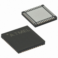
ATMEGA8515-16MU Atmel, ATMEGA8515-16MU Datasheet - Page 30

ATMEGA8515-16MU
Manufacturer Part Number
ATMEGA8515-16MU
Description
IC AVR MCU 8K 16MHZ 5V 44-QFN
Manufacturer
Atmel
Series
AVR® ATmegar
Specifications of ATMEGA8515-16MU
Core Processor
AVR
Core Size
8-Bit
Speed
16MHz
Connectivity
EBI/EMI, SPI, UART/USART
Peripherals
Brown-out Detect/Reset, POR, PWM, WDT
Number Of I /o
35
Program Memory Size
8KB (4K x 16)
Program Memory Type
FLASH
Eeprom Size
512 x 8
Ram Size
512 x 8
Voltage - Supply (vcc/vdd)
4.5 V ~ 5.5 V
Oscillator Type
Internal
Operating Temperature
-40°C ~ 85°C
Package / Case
44-VQFN Exposed Pad
Processor Series
ATMEGA8x
Core
AVR8
Data Bus Width
8 bit
Data Ram Size
512 B
Interface Type
SPI, USART
Maximum Clock Frequency
16 MHz
Number Of Programmable I/os
35
Number Of Timers
2
Operating Supply Voltage
4.5 V to 5.5 V
Maximum Operating Temperature
+ 85 C
Mounting Style
SMD/SMT
3rd Party Development Tools
EWAVR, EWAVR-BL
Development Tools By Supplier
ATAVRDRAGON, ATSTK500, ATSTK600, ATAVRISP2, ATAVRONEKIT
Minimum Operating Temperature
- 40 C
For Use With
ATAVRISP2 - PROGRAMMER AVR IN SYSTEMATSTK500 - PROGRAMMER AVR STARTER KIT
Lead Free Status / RoHS Status
Lead free / RoHS Compliant
Data Converters
-
Lead Free Status / Rohs Status
Details
- Current page: 30 of 257
- Download datasheet (2Mb)
30
ATmega8515(L)
SRAM address space is configured as one sector, the wait states are configured by the
SRW11 and SRW10 bits.
Table 2. Sector Limits with Different Settings of SRL2..0
• Bit 1 and Bit 6 MCUCR – SRW11, SRW10: Wait State Select Bits for Upper
The SRW11 and SRW10 bits control the number of wait states for the upper sector of
the External Memory address space, see Table 3.
• Bit 3..2 – SRW01, SRW00: Wait State Select Bits for Lower Sector
The SRW01 and SRW00 bits control the number of wait states for the lower sector of
the External Memory address space, see Table 3.
Table 3. Wait States
Note:
SRWn1
Sector
SRL2
0
0
1
1
0
0
0
0
1
1
1
1
1. n = 0 or 1 (lower/upper sector).
SRWn0
For further details of the timing and wait states of the External Memory Interface, see
Figure 13 to Figure 16 how the setting of the SRW bits affects the timing.
0
1
0
1
SRL1
0
0
1
1
0
0
1
1
(1)
Wait States
No wait states.
Wait one cycle during read/write strobe.
Wait two cycles during read/write strobe.
Wait two cycles during read/write and wait one cycle before driving out
new address.
SRL0
0
1
0
1
0
1
0
1
Sector Limits
Lower sector = N/A
Upper sector = 0x0260 - 0xFFFF
Lower sector = 0x0260 - 0x1FFF
Upper sector = 0x2000 - 0xFFFF
Lower sector = 0x0260 - 0x3FFF
Upper sector = 0x4000 - 0xFFFF
Lower sector = 0x0260 - 0x5FFF
Upper sector = 0x6000 - 0xFFFF
Lower sector = 0x0260 - 0x7FFF
Upper sector = 0x8000 - 0xFFFF
Lower sector = 0x0260 - 0x9FFF
Upper sector = 0xA000 - 0xFFFF
Lower sector = 0x0260 - 0xBFFF
Upper sector = 0xC000 - 0xFFFF
Lower sector = 0x0260 - 0xDFFF
Upper sector = 0xE000 - 0xFFFF
2512K–AVR–01/10
Related parts for ATMEGA8515-16MU
Image
Part Number
Description
Manufacturer
Datasheet
Request
R

Part Number:
Description:
IC AVR MCU 2.4GHZ XCEIVER 64QFN
Manufacturer:
Atmel
Datasheet:

Part Number:
Description:
Manufacturer:
Atmel
Datasheet:

Part Number:
Description:
MCU ATMEGA644/AT86RF230 40-DIP
Manufacturer:
Atmel
Datasheet:

Part Number:
Description:
BUNDLE ATMEGA644P/AT86RF230 QFN
Manufacturer:
Atmel
Datasheet:

Part Number:
Description:
BUNDLE ATMEGA644P/AT86RF230 TQFP
Manufacturer:
Atmel
Datasheet:

Part Number:
Description:
MCU ATMEGA1281/AT86RF230 64-TQFP
Manufacturer:
Atmel
Datasheet:

Part Number:
Description:
MCU ATMEGA1280/AT86RF230 100TQFP
Manufacturer:
Atmel
Datasheet:

Part Number:
Description:
BUNDLE ATMEGA1280/AT86RF100-TQFP
Manufacturer:
Atmel
Datasheet:

Part Number:
Description:
BUNDLE ATMEGA2560V/AT86RF230-ZU
Manufacturer:
Atmel
Datasheet:

Part Number:
Description:
MCU ATMEGA2561/AT86RF230 64-TQFP
Manufacturer:
Atmel
Datasheet:

Part Number:
Description:
INTERVAL AND WIPE/WASH WIPER CONTROL IC WITH DELAY
Manufacturer:
ATMEL Corporation
Datasheet:

Part Number:
Description:
Low-Voltage Voice-Switched IC for Hands-Free Operation
Manufacturer:
ATMEL Corporation
Datasheet:

Part Number:
Description:
MONOLITHIC INTEGRATED FEATUREPHONE CIRCUIT
Manufacturer:
ATMEL Corporation
Datasheet:

Part Number:
Description:
AM-FM Receiver IC U4255BM-M
Manufacturer:
ATMEL Corporation
Datasheet:


