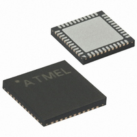
ATXMEGA16A4-MH Atmel, ATXMEGA16A4-MH Datasheet - Page 10

ATXMEGA16A4-MH
Manufacturer Part Number
ATXMEGA16A4-MH
Description
MCU AVR 16K FLASH 1.6V 44-QFN
Manufacturer
Atmel
Series
AVR® XMEGAr
Datasheet
1.ATXMEGA16A4-CUR.pdf
(108 pages)
Specifications of ATXMEGA16A4-MH
Core Processor
AVR
Core Size
8/16-Bit
Speed
32MHz
Connectivity
I²C, IrDA, SPI, UART/USART
Peripherals
Brown-out Detect/Reset, DMA, POR, PWM, WDT
Number Of I /o
34
Program Memory Size
16KB (8K x 16)
Program Memory Type
FLASH
Eeprom Size
1K x 8
Ram Size
2K x 8
Voltage - Supply (vcc/vdd)
1.6 V ~ 3.6 V
Data Converters
A/D 12x12b, D/A 2x12b
Oscillator Type
Internal
Operating Temperature
-40°C ~ 85°C
Package / Case
44-VQFN Exposed Pad
Processor Series
ATXMEGA16x
Core
AVR8
Data Bus Width
8 bit, 16 bit
Data Ram Size
2 KB
Interface Type
I2C, SPI, USART
Maximum Clock Frequency
32 MHz
Number Of Programmable I/os
36
Number Of Timers
5
Operating Supply Voltage
1.6 V to 3.6 V
Maximum Operating Temperature
+ 85 C
Mounting Style
SMD/SMT
3rd Party Development Tools
EWAVR, EWAVR-BL
Development Tools By Supplier
ATAVRDRAGON, ATAVRISP2, ATAVRONEKIT
Minimum Operating Temperature
- 40 C
On-chip Adc
12 bit, 1 Channel
On-chip Dac
2 bit, 1 Channel
Package
44VFBGA EP
Device Core
AVR
Family Name
XMEGA
Maximum Speed
32 MHz
For Use With
ATAVRONEKIT - KIT AVR/AVR32 DEBUGGER/PROGRMMRATSTK600-TQFP44 - STK600 SOCKET/ADAPTER 44-TQFP770-1007 - ISP 4PORT ATMEL AVR MCU SPI/JTAG770-1004 - ISP 4PORT FOR ATMEL AVR MCU SPIATAVRISP2 - PROGRAMMER AVR IN SYSTEM
Lead Free Status / RoHS Status
Lead free / RoHS Compliant
Other names
ATXMEGA16A4-MU
ATXMEGA16A4-MU
ATXMEGA16A4-MU
7. Memories
7.1
7.2
8069Q–AVR–12/10
Features
Overview
•
•
•
•
The AVR architecture has two main memory spaces, the Program Memory and the Data Mem-
ory. In addition, the XMEGA A4 features an EEPROM Memory for non-volatile data storage. All
three memory spaces are linear and require no paging. The available memory size configura-
tions are shown in
memory signature row for calibration data, device identification, serial number etc.
Non-volatile memory spaces can be locked for further write or read/write operations. This pre-
vents unrestricted access to the application software.
Flash Program Memory
Data Memory
Production Signature Row Memory for factory programmed data
User Signature Row
– One linear address space
– In-System Programmable
– Self-Programming and Bootloader support
– Application Section for application code
– Application Table Section for application code or data storage
– Boot Section for application code or bootloader code
– Separate lock bits and protection for all sections
– Built in fast CRC check of a selectable flash program memory section
– One linear address space
– Single cycle access from CPU
– SRAM
– EEPROM
– I/O Memory
– Bus arbitration
– Separate buses for SRAM, EEPROM, I/O Memory and External Memory access
Byte and page accessible
Optional memory mapping for direct load and store
Configuration and Status registers for all peripherals and modules
16 bit-accessible General Purpose Register for global variables or flags
Safe and deterministic handling of CPU and DMA Controller priority
Simultaneous bus access for CPU and DMA Controller
Device ID for each microcontroller device type
Serial number for each device
Oscillator calibration bytes
ADC, DAC and temperature sensor calibration data
One flash page in size
Can be read and written from software
Content is kept after chip erase
”Ordering Information” on page
2. In addition each device has a Flash
XMEGA A4
10


