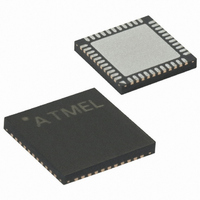
ATXMEGA16A4-MH Atmel, ATXMEGA16A4-MH Datasheet - Page 12

ATXMEGA16A4-MH
Manufacturer Part Number
ATXMEGA16A4-MH
Description
MCU AVR 16K FLASH 1.6V 44-QFN
Manufacturer
Atmel
Series
AVR® XMEGAr
Datasheet
1.ATXMEGA16A4-CUR.pdf
(108 pages)
Specifications of ATXMEGA16A4-MH
Core Processor
AVR
Core Size
8/16-Bit
Speed
32MHz
Connectivity
I²C, IrDA, SPI, UART/USART
Peripherals
Brown-out Detect/Reset, DMA, POR, PWM, WDT
Number Of I /o
34
Program Memory Size
16KB (8K x 16)
Program Memory Type
FLASH
Eeprom Size
1K x 8
Ram Size
2K x 8
Voltage - Supply (vcc/vdd)
1.6 V ~ 3.6 V
Data Converters
A/D 12x12b, D/A 2x12b
Oscillator Type
Internal
Operating Temperature
-40°C ~ 85°C
Package / Case
44-VQFN Exposed Pad
Processor Series
ATXMEGA16x
Core
AVR8
Data Bus Width
8 bit, 16 bit
Data Ram Size
2 KB
Interface Type
I2C, SPI, USART
Maximum Clock Frequency
32 MHz
Number Of Programmable I/os
36
Number Of Timers
5
Operating Supply Voltage
1.6 V to 3.6 V
Maximum Operating Temperature
+ 85 C
Mounting Style
SMD/SMT
3rd Party Development Tools
EWAVR, EWAVR-BL
Development Tools By Supplier
ATAVRDRAGON, ATAVRISP2, ATAVRONEKIT
Minimum Operating Temperature
- 40 C
On-chip Adc
12 bit, 1 Channel
On-chip Dac
2 bit, 1 Channel
Package
44VFBGA EP
Device Core
AVR
Family Name
XMEGA
Maximum Speed
32 MHz
For Use With
ATAVRONEKIT - KIT AVR/AVR32 DEBUGGER/PROGRMMRATSTK600-TQFP44 - STK600 SOCKET/ADAPTER 44-TQFP770-1007 - ISP 4PORT ATMEL AVR MCU SPI/JTAG770-1004 - ISP 4PORT FOR ATMEL AVR MCU SPIATAVRISP2 - PROGRAMMER AVR IN SYSTEM
Lead Free Status / RoHS Status
Lead free / RoHS Compliant
Other names
ATXMEGA16A4-MU
ATXMEGA16A4-MU
ATXMEGA16A4-MU
7.4
Figure 7-2.
7.4.1
7.4.2
8069Q–AVR–12/10
Byte Address
Data Memory
I/O Memory
SRAM Data Memory
2FFF
17FF
1000
2000
FFF
Data Memory Map (Hexadecimal address)
0
ATxmega64A4
Internal SRAM
I/O Registers
RESERVED
EEPROM
(4 KB)
(2 KB)
(4 KB)
The Data Memory consist of the I/O Memory, EEPROM and SRAM memories, all within one lin-
ear address space, see
devices in the family is identical and with empty, reserved memory space for smaller devices.
All peripherals and modules are addressable through I/O memory locations in the data memory
space. All I/O memory locations can be accessed by the Load (LD/LDS/LDD) and Store
(ST/STS/STD) instructions, transferring data between the 32 general purpose registers in the
CPU and the I/O Memory.
The IN and OUT instructions can address I/O memory locations in the range 0x00 - 0x3F
directly.
I/O registers within the address range 0x00 - 0x1F are directly bit-accessible using the SBI and
CBI instructions. The value of single bits can be checked by using the SBIS and SBIC instruc-
tions on these registers.
The I/O memory address for all peripherals and modules in XMEGA A4 is shown in the
eral Module Address Map” on page
The XMEGA A4 devices have internal SRAM memory for data storage.
Byte Address
Figure 7-2 on page
2FFF
13FF
1000
2000
FFF
0
53.
ATxmega32A4
Internal SRAM
I/O Registers
RESERVED
EEPROM
(4 KB)
(1 KB)
(4 KB)
12. To simplify development, the memory map for all
Byte Address
Byte Address
3FFF
17FF
1000
2000
13FF
27FF
FFF
1000
2000
FFF
0
0
XMEGA A4
ATxmega128A4
Internal SRAM
ATxmega16A4
Internal SRAM
I/O Registers
I/O Registers
RESERVED
EEPROM
RESERVED
EEPROM
(4 KB)
(2 KB)
(8 KB)
(4 KB)
(1 KB)
(2 KB)
”Periph-
12


