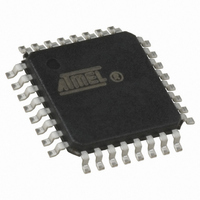
ATMEGA168-15AZ Atmel, ATMEGA168-15AZ Datasheet - Page 236

ATMEGA168-15AZ
Manufacturer Part Number
ATMEGA168-15AZ
Description
MCU AVR 16K FLASH 15MHZ 32-TQFP
Manufacturer
Atmel
Series
AVR® ATmegar
Datasheet
1.ATMEGA168-15AZ.pdf
(340 pages)
Specifications of ATMEGA168-15AZ
Package / Case
32-TQFP, 32-VQFP
Voltage - Supply (vcc/vdd)
2.7 V ~ 5.5 V
Operating Temperature
-40°C ~ 125°C
Speed
16MHz
Number Of I /o
23
Eeprom Size
512 x 8
Core Processor
AVR
Program Memory Type
FLASH
Ram Size
1K x 8
Program Memory Size
16KB (16K x 8)
Data Converters
A/D 8x10b
Oscillator Type
Internal
Peripherals
Brown-out Detect/Reset, POR, PWM, WDT
Connectivity
I²C, SPI, UART/USART
Core Size
8-Bit
Cpu Family
ATmega
Device Core
AVR
Device Core Size
8b
Frequency (max)
16MHz
Interface Type
2-Wire/USART/Serial
Total Internal Ram Size
1KB
# I/os (max)
23
Number Of Timers - General Purpose
3
Operating Supply Voltage (typ)
3.3/5V
Operating Supply Voltage (max)
5.5V
Operating Supply Voltage (min)
2.7V
On-chip Adc
8-chx10-bit
Instruction Set Architecture
RISC
Operating Temp Range
-40C to 125C
Operating Temperature Classification
Automotive
Mounting
Surface Mount
Pin Count
32
Package Type
TQFP
Lead Free Status / RoHS Status
Lead free / RoHS Compliant
Available stocks
Company
Part Number
Manufacturer
Quantity
Price
- Current page: 236 of 340
- Download datasheet (6Mb)
20.1
20.1.1
236
Analog Comparator Multiplexed Input
ATmega48/88/168 Automotive
Digital Input Disable Register 1 – DIDR1
It is possible to select any of the ADC7..0 pins to replace the negative input to the Analog Com-
parator. The ADC multiplexer is used to select this input, and consequently, the ADC must be
switched off to utilize this feature. If the Analog Comparator Multiplexer Enable bit (ACME in
ADCSRB) is set and the ADC is switched off (ADEN in ADCSRA is zero), MUX2..0 in ADMUX
select the input pin to replace the negative input to the Analog Comparator, as shown in
20-2. If ACME is cleared or ADEN is set, AIN1 is applied to the negative input to the Analog
Comparator.
Table 20-2.
• Bit 7..2 – Res: Reserved Bits
These bits are unused bits in the ATmega48/88/168, and will always read as zero.
• Bit 1, 0 – AIN1D, AIN0D: AIN1, AIN0 Digital Input Disable
When this bit is written logic one, the digital input buffer on the AIN1/0 pin is disabled. The corre-
sponding PIN Register bit will always read as zero when this bit is set. When an analog signal is
applied to the AIN1/0 pin and the digital input from this pin is not needed, this bit should be writ-
ten logic one to reduce power consumption in the digital input buffer.
Bit
Read/Write
Initial Value
ACME
0
1
1
1
1
1
1
1
1
1
Analog Comparator Multiplexed Input
ADEN
R
7
–
0
x
1
0
0
0
0
0
0
0
0
R
6
–
0
MUX2..0
000
001
010
011
100
101
110
111
xxx
xxx
R
5
–
0
Analog Comparator Negative Input
AIN1
AIN1
ADC0
ADC1
ADC2
ADC3
ADC4
ADC5
ADC6
ADC7
R
4
–
0
R
3
–
0
R
2
–
0
AIN1D
R/W
1
0
AIN0D
R/W
0
0
7530I–AVR–02/10
DIDR1
Table
Related parts for ATMEGA168-15AZ
Image
Part Number
Description
Manufacturer
Datasheet
Request
R

Part Number:
Description:
Manufacturer:
Atmel Corporation
Datasheet:

Part Number:
Description:
Manufacturer:
Atmel Corporation
Datasheet:

Part Number:
Description:
Manufacturer:
ATMEL Corporation
Datasheet:

Part Number:
Description:
IC AVR MCU 16K 20MHZ 32TQFP
Manufacturer:
Atmel
Datasheet:

Part Number:
Description:
IC AVR MCU 16K 20MHZ 32-QFN
Manufacturer:
Atmel
Datasheet:

Part Number:
Description:
IC AVR MCU 16K 20MHZ 28DIP
Manufacturer:
Atmel
Datasheet:

Part Number:
Description:
MCU AVR 16K FLASH 15MHZ 32-QFN
Manufacturer:
Atmel
Datasheet:

Part Number:
Description:
IC AVR MCU 16K 20MHZ 32TQFP
Manufacturer:
Atmel
Datasheet:

Part Number:
Description:
MCU AVR 16KB FLASH 20MHZ 32QFN
Manufacturer:
Atmel
Datasheet:

Part Number:
Description:
MCU AVR 16KB FLASH 20MHZ 32TQFP
Manufacturer:
Atmel
Datasheet:

Part Number:
Description:
IC MCU AVR 16K FLASH 32-QFN
Manufacturer:
Atmel
Datasheet:


