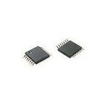
P89LPC9151FDH,129 NXP Semiconductors, P89LPC9151FDH,129 Datasheet - Page 13

P89LPC9151FDH,129
Manufacturer Part Number
P89LPC9151FDH,129
Description
IC 80C51 MCU FLASH 2KB 14TSSOP
Manufacturer
NXP Semiconductors
Series
LPC900r
Datasheet
1.P89LPC9151FDH129.pdf
(91 pages)
Specifications of P89LPC9151FDH,129
Program Memory Type
FLASH
Program Memory Size
2KB (2K x 8)
Package / Case
14-TSSOP
Core Processor
8051
Core Size
8-Bit
Speed
18MHz
Connectivity
I²C, UART/USART
Peripherals
Brown-out Detect/Reset, POR, PWM, WDT
Number Of I /o
12
Ram Size
256 x 8
Voltage - Supply (vcc/vdd)
2.4 V ~ 3.6 V
Data Converters
A/D 4x8b; D/A 1x8b
Oscillator Type
Internal
Operating Temperature
-40°C ~ 85°C
Processor Series
P89LPC
Core
80C51
Data Bus Width
8 bit
Data Ram Size
256 B
Interface Type
SPI
Maximum Clock Frequency
18 MHz
Number Of Programmable I/os
10
Number Of Timers
2
Operating Supply Voltage
2.4 V to 3.6 V
Maximum Operating Temperature
+ 85 C
Mounting Style
SMD/SMT
3rd Party Development Tools
PK51, CA51, A51, ULINK2
Minimum Operating Temperature
- 40 C
On-chip Adc
8 bit, 4 Channel
Lead Free Status / RoHS Status
Lead free / RoHS Compliant
Eeprom Size
-
Lead Free Status / Rohs Status
Lead free / RoHS Compliant
Other names
935290259129
NXP Semiconductors
Table 4.
[1]
P89LPC9151_61_71_2
Product data sheet
Symbol
P1.2/T0/SCL
P1.3/INT0/SDA
P1.5/RST
P2.2 to P2.5
P2.2/MOSI
P2.3/MISO
P2.4/SS
P2.5/SPICLK
V
V
SS
DD
Input/output for P1.0 to P1.3. Input for P1.5.
P89LPC9161 Pin description
Pin
TSSOP16
8
7
3
6
5
2
11
4
12
Type Description
I/O
I/O
I/O
I/O
I
I/O
I
I
I/O
I/O
I/O
I/O
I/O
I/O
I
I/O
I/O
I
I
P1.2 — Port 1 bit 2 (open-drain when used as output).
T0 — Timer/counter 0 external count input or overflow output (open-drain when
used as output).
SCL — I
P1.3 — Port 1 bit 3 (open-drain when used as output).
INT0 — External interrupt 0 input.
SDA — I
P1.5 — Port 1 bit 5 (input only).
RST — External Reset input during power-on or if selected via UCFG1. When
functioning as a reset input, a LOW on this pin resets the microcontroller, causing
I/O ports and peripherals to take on their default states, and the processor begins
execution at address 0. Also used during a power-on sequence to force ISP
mode.
Port 2: Port 2 is an 4-bit I/O port with a user-configurable output type. During
reset Port 2 latches are configured in the input only mode with the internal pull-up
disabled. The operation of Port 2 pins as inputs and outputs depends upon the
port configuration selected. Each port pin is configured independently. Refer to
Section 7.15 “I/O ports”
All pins have Schmitt trigger inputs.
Port 2 also provides various special functions as described below:
P2.2 — Port 2 bit 2.
MOSI — SPI master out slave in. When configured as master, this pin is output;
when configured as slave, this pin is input.
P2.3 — Port 2 bit 3.
MISO — When configured as master, this pin is input, when configured as slave,
this pin is output.
P2.4 — Port 2 bit 4.
SS — SPI Slave select.
P2.5 — Port 2 bit 5.
SPICLK — SPI clock. When configured as master, this pin is output; when
configured as slave, this pin is input.
Ground: 0 V reference.
Power supply: This is the power supply voltage for normal operation as well as
Idle and Power-down modes.
Rev. 02 — 9 February 2010
2
2
C-bus serial clock input/output.
C-bus serial data input/output.
for details.
P89LPC9151/9161/9171
8-bit microcontroller with 8-bit ADC
© NXP B.V. 2010. All rights reserved.
13 of 91


