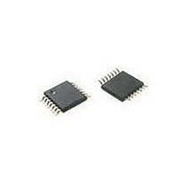
P89LPC9151FDH,129 NXP Semiconductors, P89LPC9151FDH,129 Datasheet - Page 61

P89LPC9151FDH,129
Manufacturer Part Number
P89LPC9151FDH,129
Description
IC 80C51 MCU FLASH 2KB 14TSSOP
Manufacturer
NXP Semiconductors
Series
LPC900r
Datasheet
1.P89LPC9151FDH129.pdf
(91 pages)
Specifications of P89LPC9151FDH,129
Program Memory Type
FLASH
Program Memory Size
2KB (2K x 8)
Package / Case
14-TSSOP
Core Processor
8051
Core Size
8-Bit
Speed
18MHz
Connectivity
I²C, UART/USART
Peripherals
Brown-out Detect/Reset, POR, PWM, WDT
Number Of I /o
12
Ram Size
256 x 8
Voltage - Supply (vcc/vdd)
2.4 V ~ 3.6 V
Data Converters
A/D 4x8b; D/A 1x8b
Oscillator Type
Internal
Operating Temperature
-40°C ~ 85°C
Processor Series
P89LPC
Core
80C51
Data Bus Width
8 bit
Data Ram Size
256 B
Interface Type
SPI
Maximum Clock Frequency
18 MHz
Number Of Programmable I/os
10
Number Of Timers
2
Operating Supply Voltage
2.4 V to 3.6 V
Maximum Operating Temperature
+ 85 C
Mounting Style
SMD/SMT
3rd Party Development Tools
PK51, CA51, A51, ULINK2
Minimum Operating Temperature
- 40 C
On-chip Adc
8 bit, 4 Channel
Lead Free Status / RoHS Status
Lead free / RoHS Compliant
Eeprom Size
-
Lead Free Status / Rohs Status
Lead free / RoHS Compliant
Other names
935290259129
NXP Semiconductors
P89LPC9151_61_71_2
Product data sheet
Fig 21. ADC block diagram
8.4.1 Fixed channel, single conversion mode
8.4.2 Fixed channel, continuous conversion mode
8.4.3 Auto scan, single conversion mode
8.4.4 Auto scan, continuous conversion mode
8.3 Block diagram
8.4 ADC operating modes
A single input channel can be selected for conversion. A single conversion will be
performed and the result placed in the result register which corresponds to the selected
input channel. An interrupt, if enabled, will be generated after the conversion completes.
A single input channel can be selected for continuous conversion. The results of the
conversions will be sequentially placed in the four result register. The user may select
whether an interrupt can be generated after every four conversions. Additional conversion
results will again cycle through the four result register, overwriting the previous results.
Continuous conversions continue until terminated by the user.
Any combination of the four input channels can be selected for conversion. A single
conversion of each selected input will be performed and the result placed in the result
register which corresponds to the selected input channel. An interrupt, if enabled, will be
generated after all selected channels have been converted. If only a single channel is
selected this is equivalent to single channel, single conversion mode.
Any combination of the four input channels can be selected for conversion. A conversion
of each selected input will be performed and the result placed in the result register which
corresponds to the selected input channel. An interrupt, if enabled, will be generated after
8-bit conversion time of ≥ 1.61 μs at an A/D clock of 8.0 MHz.
Interrupt or polled operation.
Boundary limits interrupt.
DAC output to a port pin with high output impedance.
Clock divider.
Power-down mode.
Edge triggered.
INPUT
MUX
Rev. 02 — 9 February 2010
comp
DAC1
P89LPC9151/9161/9171
SAR
cclk
8
8-bit microcontroller with 8-bit ADC
002aaa783
© NXP B.V. 2010. All rights reserved.
61 of 91


