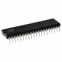
P80C32X2FN,112 NXP Semiconductors, P80C32X2FN,112 Datasheet - Page 10

P80C32X2FN,112
Manufacturer Part Number
P80C32X2FN,112
Description
IC 80C51 MCU 256 ROMLESS 40DIP
Manufacturer
NXP Semiconductors
Series
80Cr
Datasheet
1.P87C52X2BN112.pdf
(62 pages)
Specifications of P80C32X2FN,112
Core Processor
8051
Core Size
8-Bit
Speed
33MHz
Connectivity
EBI/EMI, UART/USART
Peripherals
POR
Number Of I /o
32
Program Memory Type
ROMless
Ram Size
256 x 8
Voltage - Supply (vcc/vdd)
2.7 V ~ 5.5 V
Oscillator Type
Internal
Operating Temperature
-40°C ~ 85°C
Package / Case
40-DIP (0.600", 15.24mm)
Cpu Family
80C
Device Core
80C51
Device Core Size
8b
Frequency (max)
33MHz
Interface Type
UART
Program Memory Size
Not Required
Total Internal Ram Size
256Byte
# I/os (max)
32
Number Of Timers - General Purpose
3
Operating Supply Voltage (typ)
5V
Operating Supply Voltage (max)
5.5V
Operating Supply Voltage (min)
4.5V
Instruction Set Architecture
CISC
Operating Temp Range
-40C to 85C
Operating Temperature Classification
Industrial
Mounting
Through Hole
Pin Count
40
Package Type
PDIP
Processor Series
P80C3x
Core
80C51
Data Bus Width
8 bit
Data Ram Size
256 B
Maximum Clock Frequency
33 MHz
Number Of Programmable I/os
32
Number Of Timers
3
Operating Supply Voltage
2.7 V to 5.5 V
Maximum Operating Temperature
+ 85 C
Mounting Style
Through Hole
3rd Party Development Tools
PK51, CA51, A51, ULINK2
Minimum Operating Temperature
- 40 C
Lead Free Status / RoHS Status
Lead free / RoHS Compliant
Eeprom Size
-
Program Memory Size
-
Data Converters
-
Lead Free Status / Rohs Status
Compliant
Other names
935269611112
P80C32X2FN
P80C32X2FN
P80C32X2FN
P80C32X2FN
Available stocks
Company
Part Number
Manufacturer
Quantity
Price
Company:
Part Number:
P80C32X2FN,112
Manufacturer:
HONGFA
Quantity:
16 000
Philips Semiconductors
PIN DESCRIPTIONS
2003 Jan 24
V
V
P0.0-0.7
P1.0–P1.7
P2.0–P2.7
P3.0–P3.7
RST
ALE/PROG
MNEMONIC
SS
CC
80C51 8-bit microcontroller family
4K/8K/16K/32K ROM/OTP, low voltage (2.7 to 5.5 V),
low power, high speed (30/33 MHz)
39–32 43–36
21–28 24–31
10–17
DIP
1–8
20
40
10
11
12
13
14
15
16
17
30
1
2
9
PLCC
13–19
PIN NUMBER
2–9
11,
22
44
13
14
15
16
17
18
19
10
33
11
2
3
40–44,
37–30
18–25
LQFP
7–13
1–3
16
38
40
41
10
11
12
13
27
5,
5
7
8
9
4
TSSOP
28–21
30–37
10–17
1–6
29
30
31
38
19
9
1
2
3
4
5
6
TYPE NAME AND FUNCTION
I/O
I/O
I/O
I/O
I/O
O
O
O
O
I
I
I
I
I
I
I
I
I
Ground: 0 V reference.
Power Supply: This is the power supply voltage for normal, idle, and power-down
operation.
Port 0: Port 0 is an open-drain, bidirectional I/O port. Port 0 pins that have 1s
written to them float and can be used as high-impedance inputs. Port 0 is also the
multiplexed low-order address and data bus during accesses to external program
and data memory. In this application, it uses strong internal pull-ups when emitting
1s. Port 0 also outputs the code bytes during program verification and received
code bytes during EPROM programming. External pull-ups are required during
program verification.
Port 1: Port 1 is an 8-bit bidirectional I/O port with internal pull-ups. Port 1 pins that
have 1s written to them are pulled high by the internal pull-ups and can be used as
inputs. As inputs, port 1 pins that are externally pulled low will source current
because of the internal pull-ups. (See DC Electrical Characteristics: I
receives the low-order address byte during program memory verification. Alternate
functions for Port 1 include:
Port 2: Port 2 is an 8-bit bidirectional I/O port with internal pull-ups. Port 2 pins that
have 1s written to them are pulled high by the internal pull-ups and can be used as
inputs. As inputs, port 2 pins that are externally being pulled low will source current
because of the internal pull-ups. (See DC Electrical Characteristics: I
emits the high-order address byte during fetches from external program memory
and during accesses to external data memory that use 16-bit addresses (MOVX
@DPTR). In this application, it uses strong internal pull-ups when emitting 1s.
During accesses to external data memory that use 8-bit addresses (MOV @Ri), port
2 emits the contents of the P2 special function register. Some Port 2 pins receive
the high order address bits during EPROM programming and verification.
Port 3: Port 3 is an 8-bit bidirectional I/O port with internal pull-ups. Port 3 pins that
have 1s written to them are pulled high by the internal pull-ups and can be used as
inputs. As inputs, port 3 pins that are externally being pulled low will source current
because of the pull-ups. (See DC Electrical Characteristics: I
the special features of the 80C51 family, as listed below:
Reset: A high on this pin for two machine cycles while the oscillator is running,
resets the device. An internal diffused resistor to V
using only an external capacitor to V
Address Latch Enable/Program Pulse: Output pulse for latching the low byte of
the address during an access to external memory. In normal operation, ALE is
emitted at a constant rate of 1/6 (12-clock Mode) or 1/3 (6-clock Mode) the
oscillator frequency, and can be used for external timing or clocking. Note that one
ALE pulse is skipped during each access to external data memory. This pin is also
the program pulse input (PROG) during EPROM programming. ALE can be
disabled by setting SFR auxiliary.0. With this bit set, ALE will be active only during
a MOVX instruction.
T2 (P1.0): Timer/Counter 2 external count input/clockout (see Programmable
Clock-Out)
T2EX (P1.1): Timer/Counter 2 Reload/Capture/Direction control
RxD (P3.0): Serial input port
TxD (P3.1): Serial output port
INT0 (P3.2): External interrupt
INT1 (P3.3): External interrupt
T0 (P3.4): Timer 0 external input
T1 (P3.5): Timer 1 external input
WR (P3.6): External data memory write strobe
RD (P3.7): External data memory read strobe
10
1
1
CC
.
P80C3xX2; P80C5xX2;
SS
permits a power-on reset
IL
). Port 3 also serves
P87C5xX2
IL
IL
). Port 1 also
). Port 2
Product data


