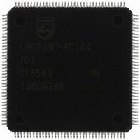
LPC2290FBD144/01,5 NXP Semiconductors, LPC2290FBD144/01,5 Datasheet - Page 13

LPC2290FBD144/01,5
Manufacturer Part Number
LPC2290FBD144/01,5
Description
IC ARM7 MCU RAM 16K 144-LQFP
Manufacturer
NXP Semiconductors
Series
LPC2200r
Datasheet
1.LPC2290FBD144015.pdf
(41 pages)
Specifications of LPC2290FBD144/01,5
Package / Case
144-LQFP
Core Processor
ARM7
Core Size
16/32-Bit
Speed
60MHz
Connectivity
CAN, EBI/EMI, I²C, Microwire, SPI, SSI, SSP, UART/USART
Peripherals
PWM, WDT
Number Of I /o
76
Program Memory Type
ROMless
Ram Size
64K x 8
Voltage - Supply (vcc/vdd)
1.65 V ~ 3.6 V
Data Converters
A/D 8x10b
Oscillator Type
Internal
Operating Temperature
-40°C ~ 85°C
Processor Series
LPC22
Core
ARM7TDMI-S
Data Bus Width
16 bit, 32 bit
Data Ram Size
64 KB
Interface Type
CAN/I2C/SPI/UART
Maximum Clock Frequency
72 MHz
Number Of Programmable I/os
76
Number Of Timers
2
Operating Supply Voltage
3.3 V
Maximum Operating Temperature
+ 85 C
Mounting Style
SMD/SMT
3rd Party Development Tools
MDK-ARM, RL-ARM, ULINK2
Minimum Operating Temperature
- 40 C
On-chip Adc
8-ch x 10-bit
Package
144LQFP
Device Core
ARM7TDMI-S
Family Name
LPC2000
Maximum Speed
72 MHz
Lead Free Status / RoHS Status
Lead free / RoHS Compliant
For Use With
OM10091 - KIT DEV PHYCORE-ARM7/LPC2220568-1757 - BOARD EVAL FOR LPC220X ARM MCU
Eeprom Size
-
Program Memory Size
-
Lead Free Status / Rohs Status
Lead free / RoHS Compliant
Other names
568-4013
935282079551
LPC2290FBD144/01-S
935282079551
LPC2290FBD144/01-S
Available stocks
Company
Part Number
Manufacturer
Quantity
Price
Company:
Part Number:
LPC2290FBD144/01,5
Manufacturer:
NXP Semiconductors
Quantity:
10 000
NXP Semiconductors
Table 3.
[1]
[2]
[3]
[4]
[5]
[6]
[7]
LPC2290_3
Product data sheet
Symbol
V
V
V
V
V
SSA(PLL)
DD(1V8)
DDA(1V8)
DD(3V3)
DDA(3V3)
5 V tolerant pad providing digital I/O functions with TTL levels and hysteresis and 10 ns slew rate control.
5 V tolerant pad providing digital I/O functions with TTL levels and hysteresis and 10 ns slew rate control. If configured for an input
function, this pad utilizes built-in glitch filter that blocks pulses shorter than 3 ns.
Open-drain 5 V tolerant digital I/O I
functionality.
5 V tolerant pad providing digital I/O (with TTL levels and hysteresis and 10 ns slew rate control) and analog input function. If configured
for a digital input function, this pad utilizes built-in glitch filter that blocks pulses shorter than 3 ns. When configured as an ADC input,
digital section of the pad is disabled.
5 V tolerant pad with built-in pull-up resistor providing digital I/O functions with TTL levels and hysteresis and 10 ns slew rate control.
The pull-up resistor’s value ranges from 60 k to 300 k .
5 V tolerant pad providing digital input (with TTL levels and hysteresis) function only.
Pad provides special analog functionality.
Pin description
Pin
138
37, 110
143
2, 31, 39, 51,
57, 77, 94,
104, 112, 119
14
…continued
Type
I
I
I
I
I
2
C-bus 400 kHz specification compatible pad. It requires external pull-up to provide an output
Description
PLL analog ground: 0 V reference. This should nominally be the same
voltage as V
1.8 V core power supply: This is the power supply voltage for internal
circuitry.
Analog 1.8 V core power supply: This is the power supply voltage for
internal circuitry. This should be nominally the same voltage as V
should be isolated to minimize noise and error.
3.3 V pad power supply: This is the power supply voltage for the I/O ports.
Analog 3.3 V pad power supply: This should be nominally the same voltage
as V
Rev. 03 — 16 November 2006
DD(3V3)
16/32-bit ARM microcontroller with external memory interface
but should be isolated to minimize noise and error.
SS
, but should be isolated to minimize noise and error.
LPC2290
© NXP B.V. 2006. All rights reserved.
DD(1V8)
13 of 41
but


