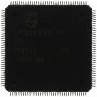
LPC2290FBD144/01,5 NXP Semiconductors, LPC2290FBD144/01,5 Datasheet - Page 17

LPC2290FBD144/01,5
Manufacturer Part Number
LPC2290FBD144/01,5
Description
IC ARM7 MCU RAM 16K 144-LQFP
Manufacturer
NXP Semiconductors
Series
LPC2200r
Datasheet
1.LPC2290FBD144015.pdf
(41 pages)
Specifications of LPC2290FBD144/01,5
Package / Case
144-LQFP
Core Processor
ARM7
Core Size
16/32-Bit
Speed
60MHz
Connectivity
CAN, EBI/EMI, I²C, Microwire, SPI, SSI, SSP, UART/USART
Peripherals
PWM, WDT
Number Of I /o
76
Program Memory Type
ROMless
Ram Size
64K x 8
Voltage - Supply (vcc/vdd)
1.65 V ~ 3.6 V
Data Converters
A/D 8x10b
Oscillator Type
Internal
Operating Temperature
-40°C ~ 85°C
Processor Series
LPC22
Core
ARM7TDMI-S
Data Bus Width
16 bit, 32 bit
Data Ram Size
64 KB
Interface Type
CAN/I2C/SPI/UART
Maximum Clock Frequency
72 MHz
Number Of Programmable I/os
76
Number Of Timers
2
Operating Supply Voltage
3.3 V
Maximum Operating Temperature
+ 85 C
Mounting Style
SMD/SMT
3rd Party Development Tools
MDK-ARM, RL-ARM, ULINK2
Minimum Operating Temperature
- 40 C
On-chip Adc
8-ch x 10-bit
Package
144LQFP
Device Core
ARM7TDMI-S
Family Name
LPC2000
Maximum Speed
72 MHz
Lead Free Status / RoHS Status
Lead free / RoHS Compliant
For Use With
OM10091 - KIT DEV PHYCORE-ARM7/LPC2220568-1757 - BOARD EVAL FOR LPC220X ARM MCU
Eeprom Size
-
Program Memory Size
-
Lead Free Status / Rohs Status
Lead free / RoHS Compliant
Other names
568-4013
935282079551
LPC2290FBD144/01-S
935282079551
LPC2290FBD144/01-S
Available stocks
Company
Part Number
Manufacturer
Quantity
Price
Company:
Part Number:
LPC2290FBD144/01,5
Manufacturer:
NXP Semiconductors
Quantity:
10 000
NXP Semiconductors
LPC2290_3
Product data sheet
6.7.1 Features
6.5 Pin connect block
6.6 External memory controller
6.7 General purpose parallel I/O and Fast I/O
Table 4.
The pin connect block allows selected pins of the microcontroller to have more than one
function. Configuration registers control the multiplexers to allow connection between the
pin and the on-chip peripherals. Peripherals should be connected to the appropriate pins
prior to being activated, and prior to any related interrupt(s) being enabled. Activity of any
enabled peripheral function that is not mapped to a related pin should be considered
undefined.
The external Static Memory Controller is a module which provides an interface between
the system bus and external (off-chip) memory devices. It provides support for up to four
independently configurable memory banks (16 MB each with byte lane enable control)
simultaneously. Each memory bank is capable of supporting SRAM, ROM, flash EPROM,
burst ROM memory, or some external I/O devices.
Each memory bank may be 8-bit, 16-bit, or 32-bit wide.
Device pins that are not connected to a specific peripheral function are controlled by the
GPIO registers. Pins may be dynamically configured as inputs or outputs. Separate
registers allow setting or clearing any number of outputs simultaneously. The value of the
output register may be read back, as well as the current state of the port pins.
Block
SPI1/SSP
PLL
RTC
System Control
A/D
CAN
•
•
Direction control of individual bits.
Separate control of output set and clear.
Interrupt sources
Flag(s)
Source: SPI1 SPI Interrupt Flag (SPIF), Mode Fault (MODF) 11
Source: SSP (available in LPC2290/01 only)
TX FIFO at least half empty (TXRIS)
RX FIFO at least half full (RXRIS)
Receive Timeout condition (RTRIS)
Receive Overrun (RORRIS)
PLL Lock (PLOCK)
RTCCIF (Counter Increment), RTCALF (Alarm)
External Interrupt 0 (EINT0)
External Interrupt 1 (EINT1)
External Interrupt 2 (EINT2)
External Interrupt 3 (EINT3)
ADC
1 ORed CAN Acceptance Filter
CAN1 (TX int, RX int)
CAN2 (TX int, RX int)
Rev. 03 — 16 November 2006
16/32-bit ARM microcontroller with external memory interface
…continued
LPC2290
© NXP B.V. 2006. All rights reserved.
VIC channel #
12
13
14
15
16
17
18
19
20, 21
22, 23
17 of 41


