LPC2290FBD144/01,5 NXP Semiconductors, LPC2290FBD144/01,5 Datasheet - Page 24
LPC2290FBD144/01,5
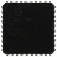
Manufacturer Part Number
LPC2290FBD144/01,5
Description
IC ARM7 MCU RAM 16K 144-LQFP
Manufacturer
NXP Semiconductors
Series
LPC2200r
Datasheet
1.LPC2290FBD144015.pdf
(41 pages)
Specifications of LPC2290FBD144/01,5
Package / Case
144-LQFP
Core Processor
ARM7
Core Size
16/32-Bit
Speed
60MHz
Connectivity
CAN, EBI/EMI, I²C, Microwire, SPI, SSI, SSP, UART/USART
Peripherals
PWM, WDT
Number Of I /o
76
Program Memory Type
ROMless
Ram Size
64K x 8
Voltage - Supply (vcc/vdd)
1.65 V ~ 3.6 V
Data Converters
A/D 8x10b
Oscillator Type
Internal
Operating Temperature
-40°C ~ 85°C
Processor Series
LPC22
Core
ARM7TDMI-S
Data Bus Width
16 bit, 32 bit
Data Ram Size
64 KB
Interface Type
CAN/I2C/SPI/UART
Maximum Clock Frequency
72 MHz
Number Of Programmable I/os
76
Number Of Timers
2
Operating Supply Voltage
3.3 V
Maximum Operating Temperature
+ 85 C
Mounting Style
SMD/SMT
3rd Party Development Tools
MDK-ARM, RL-ARM, ULINK2
Minimum Operating Temperature
- 40 C
On-chip Adc
8-ch x 10-bit
Package
144LQFP
Device Core
ARM7TDMI-S
Family Name
LPC2000
Maximum Speed
72 MHz
Lead Free Status / RoHS Status
Lead free / RoHS Compliant
For Use With
OM10091 - KIT DEV PHYCORE-ARM7/LPC2220568-1757 - BOARD EVAL FOR LPC220X ARM MCU
Eeprom Size
-
Program Memory Size
-
Lead Free Status / Rohs Status
Lead free / RoHS Compliant
Other names
568-4013
935282079551
LPC2290FBD144/01-S
935282079551
LPC2290FBD144/01-S
Available stocks
Company
Part Number
Manufacturer
Quantity
Price
Company:

Part Number:
LPC2290FBD144/01,5
Manufacturer:
NXP Semiconductors
Quantity:
10 000


NXP Semiconductors
LPC2290_3
Product data sheet
6.18.4 External interrupt inputs
6.18.5 Memory mapping control
6.18.6 Power control
6.18.7 APB bus
The Wake-up Timer monitors the crystal oscillator as the means of checking whether it is
safe to begin code execution. When power is applied to the chip, or some event caused
the chip to exit Power-down mode, some time is required for the oscillator to produce a
signal of sufficient amplitude to drive the clock logic. The amount of time depends on
many factors, including the rate of V
and its electrical characteristics (if a quartz crystal is used), as well as any other external
circuitry (e.g. capacitors), and the characteristics of the oscillator itself under the existing
ambient conditions.
The LPC2290 include up to nine edge or level sensitive External Interrupt Inputs as
selectable pin functions. When the pins are combined, external events can be processed
as four independent interrupt signals. The External Interrupt Inputs can optionally be used
to wake up the processor from Power-down mode.
The Memory Mapping Control alters the mapping of the interrupt vectors that appear
beginning at address 0x0000 0000. Vectors may be mapped to the bottom of the on-chip
flash memory, or to the on-chip static RAM. This allows code running in different memory
spaces to have control of the interrupts.
The LPC2290 support two reduced power modes: Idle mode and Power-down mode. In
Idle mode, execution of instructions is suspended until either a reset or interrupt occurs.
Peripheral functions continue operation during Idle mode and may generate interrupts to
cause the processor to resume execution. Idle mode eliminates power used by the
processor itself, memory systems and related controllers, and internal buses.
In Power-down mode, the oscillator is shut down and the chip receives no internal clocks.
The processor state and registers, peripheral registers, and internal SRAM values are
preserved throughout Power-down mode and the logic levels of chip output pins remain
static. The Power-down mode can be terminated and normal operation resumed by either
a reset or certain specific interrupts that are able to function without clocks. Since all
dynamic operation of the chip is suspended, Power-down mode reduces chip power
consumption to nearly zero.
A Power Control for Peripherals feature allows individual peripherals to be turned off if
they are not needed in the application, resulting in additional power savings.
The APB divider determines the relationship between the processor clock (CCLK) and the
clock used by peripheral devices (PCLK). The APB divider serves two purposes. The first
is to provide peripherals with the desired PCLK via APB bus so that they can operate at
the speed chosen for the ARM processor. In order to achieve this, the APB bus may be
slowed down to
properly at power-up (and its timing cannot be altered if it does not work since the APB
divider control registers reside on the APB bus), the default condition at reset is for the
APB bus to run at
is to allow power savings when an application does not require any peripherals to run at
the full processor rate. Because the APB divider is connected to the PLL output, the PLL
remains active (if it was running) during Idle mode.
1
2
1
to
4
Rev. 03 — 16 November 2006
of the processor clock rate. The second purpose of the APB divider
1
4
16/32-bit ARM microcontroller with external memory interface
of the processor clock rate. Because the APB bus must work
DD
ramp (in the case of power-on), the type of crystal
LPC2290
© NXP B.V. 2006. All rights reserved.
24 of 41
Related parts for LPC2290FBD144/01,5
Image
Part Number
Description
Manufacturer
Datasheet
Request
R

Part Number:
Description:
NXP Semiconductors designed the LPC2420/2460 microcontroller around a 16-bit/32-bitARM7TDMI-S CPU core with real-time debug interfaces that include both JTAG andembedded trace
Manufacturer:
NXP Semiconductors
Datasheet:

Part Number:
Description:
NXP Semiconductors designed the LPC2458 microcontroller around a 16-bit/32-bitARM7TDMI-S CPU core with real-time debug interfaces that include both JTAG andembedded trace
Manufacturer:
NXP Semiconductors
Datasheet:
Part Number:
Description:
NXP Semiconductors designed the LPC2468 microcontroller around a 16-bit/32-bitARM7TDMI-S CPU core with real-time debug interfaces that include both JTAG andembedded trace
Manufacturer:
NXP Semiconductors
Datasheet:
Part Number:
Description:
NXP Semiconductors designed the LPC2470 microcontroller, powered by theARM7TDMI-S core, to be a highly integrated microcontroller for a wide range ofapplications that require advanced communications and high quality graphic displays
Manufacturer:
NXP Semiconductors
Datasheet:
Part Number:
Description:
NXP Semiconductors designed the LPC2478 microcontroller, powered by theARM7TDMI-S core, to be a highly integrated microcontroller for a wide range ofapplications that require advanced communications and high quality graphic displays
Manufacturer:
NXP Semiconductors
Datasheet:
Part Number:
Description:
The Philips Semiconductors XA (eXtended Architecture) family of 16-bit single-chip microcontrollers is powerful enough to easily handle the requirements of high performance embedded applications, yet inexpensive enough to compete in the market for hi
Manufacturer:
NXP Semiconductors
Datasheet:
Part Number:
Description:
The XA-S3 device is a member of Philips Semiconductors? XA(eXtended Architecture) family of high performance 16-bitsingle-chip microcontrollers
Manufacturer:
NXP Semiconductors
Datasheet:

Part Number:
Description:
The NXP BlueStreak LH75401/LH75411 family consists of two low-cost 16/32-bit System-on-Chip (SoC) devices
Manufacturer:
NXP Semiconductors
Datasheet:
Part Number:
Description:
The NXP LPC3130/3131 combine an 180 MHz ARM926EJ-S CPU core, high-speed USB2
Manufacturer:
NXP Semiconductors
Datasheet:
Part Number:
Description:
The NXP LPC3141 combine a 270 MHz ARM926EJ-S CPU core, High-speed USB 2
Manufacturer:
NXP Semiconductors
Part Number:
Description:
The NXP LPC3143 combine a 270 MHz ARM926EJ-S CPU core, High-speed USB 2
Manufacturer:
NXP Semiconductors

Part Number:
Description:
The NXP LPC3152 combines an 180 MHz ARM926EJ-S CPU core, High-speed USB 2
Manufacturer:
NXP Semiconductors
Part Number:
Description:
The NXP LPC3154 combines an 180 MHz ARM926EJ-S CPU core, High-speed USB 2
Manufacturer:
NXP Semiconductors