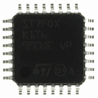
ST7FOXK1T6 STMicroelectronics, ST7FOXK1T6 Datasheet - Page 188

ST7FOXK1T6
Manufacturer Part Number
ST7FOXK1T6
Description
IC MCU 8BIT 1V FLASH MEM 32LQFP
Manufacturer
STMicroelectronics
Series
ST7r
Datasheet
1.ST7FOXF1M6.pdf
(226 pages)
Specifications of ST7FOXK1T6
Core Processor
ST7
Core Size
8-Bit
Speed
8MHz
Connectivity
I²C
Peripherals
LVD, POR, PWM, WDT
Number Of I /o
24
Program Memory Size
4KB (4K x 8)
Program Memory Type
FLASH
Ram Size
384 x 8
Voltage - Supply (vcc/vdd)
4.5 V ~ 5.5 V
Data Converters
A/D 10x10b
Oscillator Type
Internal
Operating Temperature
-40°C ~ 85°C
Package / Case
32-LQFP
Processor Series
ST7FOXx
Core
ST7
Data Bus Width
8 bit
Data Ram Size
384 B
Interface Type
I2C
Maximum Clock Frequency
8 MHz
Number Of Programmable I/os
24
Number Of Timers
4
Maximum Operating Temperature
+ 85 C
Mounting Style
SMD/SMT
Development Tools By Supplier
ST7FLITE-SK/RAIS, STX-RLINK
Minimum Operating Temperature
- 40 C
On-chip Adc
10 bit, 1 Channel
For Use With
497-5049 - KIT STARTER RAISONANCE ST7FLITE
Lead Free Status / RoHS Status
Lead free / RoHS Compliant
Eeprom Size
-
Lead Free Status / Rohs Status
Details
Other names
497-6336
Available stocks
Company
Part Number
Manufacturer
Quantity
Price
Company:
Part Number:
ST7FOXK1T6
Manufacturer:
STMicroelectronics
Quantity:
10 000
Company:
Part Number:
ST7FOXK1T6TR
Manufacturer:
STMicroelectronics
Quantity:
10 000
Electrical characteristics
12.2
188/226
Figure 82. Pin input voltage
Absolute maximum ratings
Stresses above those listed as “absolute maximum ratings” may cause permanent damage
to the device. This is a stress rating only and functional operation of the device under these
conditions is not implied. Exposure to maximum rating conditions for extended periods may
affect device reliability.
Table 66.
1. Directly connecting the RESET and I/O pins to V
2. I
internal reset is generated or an unexpected change of the I/O configuration occurs (for example, due to a
corrupted Program Counter). To guarantee safe operation, this connection has to be done through a pull-
up or pull-down resistor (typical: 4.7 kΩ for RESET, 10 kΩ for I/Os). Unused I/O pins must be tied in the
same way to V
cannot be respected, the injection current must be limited externally to the I
injection is induced by V
pads, there is no positive injection current, and the corresponding V
INJ(PIN)
V
V
V
Symbol
ESD(HBM)
ESD(CDM)
DD
V
- V
IN
must never be exceeded. This is implicitly insured if V
SS
Voltage characteristics
DD
or V
Electrostatic discharge voltage (Charge Device
Electrostatic discharge voltage (Human Body
SS
IN
according to their reset configuration.
>V
DD
Input voltage on any pin
while a negative injection is induced by V
V
Supply voltage
IN
Ratings
model)
model)
DD
or V
SS
ST7 PIN
(1)(2)
could damage the device if an unintentional
IN
ST7FOXF1, ST7FOXK1, ST7FOXK2
maximum is respected. If V
IN
maximum must always be respected
IN
V
<V
INJ(PIN)
Maximum value
see
SS
SS
-0.3 to V
. For true open-drain
Section 12.8.3 on page
value. A positive
7.0
DD
203
IN
+0.3
maximum
Unit
V


