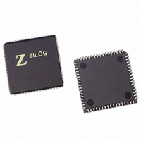
Z8F2422VS020SG Zilog, Z8F2422VS020SG Datasheet - Page 161

Z8F2422VS020SG
Manufacturer Part Number
Z8F2422VS020SG
Description
IC ENCORE MCU FLASH 24K 68PLCC
Manufacturer
Zilog
Series
Encore!® XP®r
Specifications of Z8F2422VS020SG
Core Processor
Z8
Core Size
8-Bit
Speed
20MHz
Connectivity
I²C, IrDA, SPI, UART/USART
Peripherals
Brown-out Detect/Reset, DMA, POR, PWM, WDT
Number Of I /o
46
Program Memory Size
24KB (24K x 8)
Program Memory Type
FLASH
Ram Size
2K x 8
Voltage - Supply (vcc/vdd)
3 V ~ 3.6 V
Data Converters
A/D 12x10b
Oscillator Type
Internal
Operating Temperature
0°C ~ 70°C
Package / Case
68-LCC (J-Lead)
Processor Series
Z8F242x
Core
eZ8
Data Bus Width
8 bit
Data Ram Size
2 KB
Interface Type
I2C, SPI, UART
Maximum Clock Frequency
20 MHz
Number Of Programmable I/os
46
Number Of Timers
4
Operating Supply Voltage
3 V to 3.6 V
Maximum Operating Temperature
+ 70 C
Mounting Style
SMD/SMT
Development Tools By Supplier
Z8F64200100KITG, ZENETSC0100ZACG, ZUSBSC00100ZACG, Z8F64210100ZDA, Z8F64210100ZDP, Z8F64210100ZDV, Z8F64220100ZDA, Z8F64220100ZDV, Z8F6422AR00ZEM, Z8F6422VS00ZEM, Z8F6421AN00ZEM
Minimum Operating Temperature
0 C
On-chip Adc
10 bit, 12 Channel
Lead Free Status / RoHS Status
Lead free / RoHS Compliant
Eeprom Size
-
Lead Free Status / Rohs Status
Details
Other names
269-4253
Z8F2422VS020SG
Z8F2422VS020SG
Available stocks
Company
Part Number
Manufacturer
Quantity
Price
- Current page: 161 of 297
- Download datasheet (9Mb)
PS019921-0308
Write Transaction with a 10-Bit Address
7. The I
8. After one bit of address is shifted out by the SDA signal, the Transmit interrupt is
9. Software responds by writing the second byte of address into the contents of the I
10. The I
11. If the I
12. The I
13. The I
14. Software responds by setting the STOP bit in the I
15. Software polls the STOP bit of the I
16. Software checks the ACK bit of the I
Figure 30
indicate data transferred from the I
data transferred from the slaves to the I
S
Slave Address
Figure 30. 10-Bit Addressed Slave Data Transfer Format
register.
asserted.
Data register.
signal.
high period of SCL the I
Continue with
If the slave does not acknowledge the first address byte, the I
NCKI bit and clears the ACK bit in the I
Not Acknowledge interrupt by setting the STOP and FLUSH bits and clearing the TXI
bit. The I
NCKI bits. The transaction is complete (ignore following steps).
register (2nd byte of address).
bit has been sent, the Transmit interrupt is asserted.
be cleared at the same time.
bit when the transaction is completed (STOP condition has been sent).
ACK bit is = 1. If the slave does not acknowledge, the ACK bit is = 0. The NCKI
interrupt do not occur because the STOP bit was set.
1st 7 bits
2
2
2
2
displays the data transfer format for a 10-bit addressed slave. Shaded regions
C Controller loads the I
C Controller shifts the rest of the first byte of address and write bit out the SDA
C Controller loads the I
C Controller shifts the second address byte out the SDA signal. After the first
2
C slave sends an acknowledge by pulling the SDA signal low during the next
2
C Controller sends the STOP condition on the bus and clears the STOP and
step
W = 0 A
12.
2
C Controller sets the ACK bit in the I
2
2
2
C Shift register with the contents of the I
C Shift register with the contents of the I
C Controller to slaves and unshaded regions indicate
Slave Address
2
2
C Controller.
C Control register. Hardware deasserts the STOP
2
2nd Byte
C Status register. If the slave acknowledged, the
2
C Status register. Software responds to the
2
C Control register. The TXI bit can
Z8 Encore! XP
A Data A Data A/A P/S
Product Specification
2
C Controller sets the
2
C Status register.
®
F64XX Series
2
2
C Data
C Data
I2C Controller
2
C
147
Related parts for Z8F2422VS020SG
Image
Part Number
Description
Manufacturer
Datasheet
Request
R

Part Number:
Description:
Communication Controllers, ZILOG INTELLIGENT PERIPHERAL CONTROLLER (ZIP)
Manufacturer:
Zilog, Inc.
Datasheet:

Part Number:
Description:
KIT DEV FOR Z8 ENCORE 16K TO 64K
Manufacturer:
Zilog
Datasheet:

Part Number:
Description:
KIT DEV Z8 ENCORE XP 28-PIN
Manufacturer:
Zilog
Datasheet:

Part Number:
Description:
DEV KIT FOR Z8 ENCORE 8K/4K
Manufacturer:
Zilog
Datasheet:

Part Number:
Description:
KIT DEV Z8 ENCORE XP 28-PIN
Manufacturer:
Zilog
Datasheet:

Part Number:
Description:
DEV KIT FOR Z8 ENCORE 4K TO 8K
Manufacturer:
Zilog
Datasheet:

Part Number:
Description:
CMOS Z8 microcontroller. ROM 16 Kbytes, RAM 256 bytes, speed 16 MHz, 32 lines I/O, 3.0V to 5.5V
Manufacturer:
Zilog, Inc.
Datasheet:

Part Number:
Description:
Low-cost microcontroller. 512 bytes ROM, 61 bytes RAM, 8 MHz
Manufacturer:
Zilog, Inc.
Datasheet:

Part Number:
Description:
Z8 4K OTP Microcontroller
Manufacturer:
Zilog, Inc.
Datasheet:

Part Number:
Description:
CMOS SUPER8 ROMLESS MCU
Manufacturer:
Zilog, Inc.
Datasheet:

Part Number:
Description:
SL1866 CMOSZ8 OTP Microcontroller
Manufacturer:
Zilog, Inc.
Datasheet:

Part Number:
Description:
SL1866 CMOSZ8 OTP Microcontroller
Manufacturer:
Zilog, Inc.
Datasheet:

Part Number:
Description:
OTP (KB) = 1, RAM = 125, Speed = 12, I/O = 14, 8-bit Timers = 2, Comm Interfaces Other Features = Por, LV Protect, Voltage = 4.5-5.5V
Manufacturer:
Zilog, Inc.
Datasheet:

Part Number:
Description:
Manufacturer:
Zilog, Inc.
Datasheet:


