MC56F8011VFAE Freescale Semiconductor, MC56F8011VFAE Datasheet - Page 94
MC56F8011VFAE
Manufacturer Part Number
MC56F8011VFAE
Description
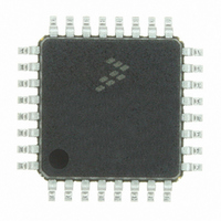
IC DIGITAL SIGNAL CTLR 32-LQFP
Manufacturer
Freescale Semiconductor
Series
56F8xxxr
Datasheet
1.MC56F8013VFAE.pdf
(126 pages)
Specifications of MC56F8011VFAE
Core Processor
56800
Core Size
16-Bit
Speed
32MHz
Connectivity
I²C, SCI, SPI
Peripherals
POR, PWM, WDT
Number Of I /o
26
Program Memory Size
12KB (6K x 16)
Program Memory Type
FLASH
Ram Size
1K x 16
Voltage - Supply (vcc/vdd)
3 V ~ 3.6 V
Data Converters
A/D 6x12b
Oscillator Type
Internal
Operating Temperature
-40°C ~ 105°C
Package / Case
32-LQFP
Product
DSCs
Data Bus Width
16 bit
Processor Series
MC56F80xx
Core
56800E
Numeric And Arithmetic Format
Fixed-Point
Device Million Instructions Per Second
32 MIPs
Maximum Clock Frequency
32 MHz
Number Of Programmable I/os
26
Data Ram Size
2 KB
Operating Supply Voltage
3.3 V
Maximum Operating Temperature
+ 105 C
Mounting Style
SMD/SMT
Development Tools By Supplier
MC56F8037EVM, DEMO56F8014-EE, DEMO56F8013-EE
Interface Type
SCI, SPI, I2C
Minimum Operating Temperature
- 40 C
For Use With
CPA56F8013 - BOARD SOCKET FOR MC56F8013APMOTOR56F8000E - KIT DEMO MOTOR CTRL SYSTEM
Lead Free Status / RoHS Status
Lead free / RoHS Compliant
Eeprom Size
-
Lead Free Status / Rohs Status
Lead free / RoHS Compliant
Available stocks
Company
Part Number
Manufacturer
Quantity
Price
Company:

Part Number:
MC56F8011VFAE
Manufacturer:
Freescale
Quantity:
1
Company:
Part Number:
MC56F8011VFAE
Manufacturer:
Freescale Semiconductor
Quantity:
10 000


1. Pin Group 3 can tolerate 6V for less than 5 seconds when they are configured as ADC inputs or during reset. Pin Group 3 can
2. Continuous input current per pin is -2 mA
94
Supply Voltage Range
Analog Supply Voltage Range
ADC High Voltage Reference
Voltage difference V
Voltage difference V
Input Voltage Range (Digital inputs)
Input Voltage Range (ADC inputs)
Input clamp current, per pin (V
Output clamp current, per pin (V
Output Voltage Range
(Normal Push-Pull mode)
Output Voltage Range
(Open Drain mode)
Ambient Temperature (Automotive)
Ambient Temperature (Industrial)
Junction Temperature (Automotive)
Junction Temperature (Industrial)
Storage Temperature (Automotive)
Storage Temperature (Industrial)
tolerate 6V if they are configured as GPIO.
Characteristic
DD
SS
to V
to V
This device contains protective circuitry to guard
against damage due to high static voltage or electrical
fields. However, normal precautions are advised to
avoid
maximum-rated voltages to this high-impedance circuit.
Reliability of operation is enhanced if unused inputs are
tied to an appropriate voltage level.
SSA
DDA
IN
O
< 0)
1
< 0)
Table 10-1 Absolute Maximum Ratings
application
2
2
56F8013/56F8011 Data Sheet, Rev. 12
(V
Symbol
V
V
ΔV
V
ΔV
V
T
T
OUTOD
V
V
SS
V
of
REFH
V
V
T
T
DDA
OUT
T
T
STG
STG
INA
DD
OC
IN
IC
CAUTION
A
A
DD
SS
J
J
= 0V, V
any
SSA
voltages
= 0V)
Pin Groups 1, 2
Pin Groups 1, 2
Pin Group 3
Pin Group 1
Notes
higher
- 0.3
- 0.3
- 0.3
- 0.3
- 0.3
- 0.3
Min
-0.3
-0.3
-0.3
-40
-40
-40
-40
-55
-55
-
-
than
Freescale Semiconductor
Max
125
105
150
125
150
150
4.0
4.0
4.0
0.3
0.3
6.0
4.0
-20
-20
4.0
6.0
Unit
mA
mA
°C
°C
°C
°C
°C
°C
V
V
V
V
V
V
V
V
V
Related parts for MC56F8011VFAE
Image
Part Number
Description
Manufacturer
Datasheet
Request
R

Part Number:
Description:
16-bit Digital Signal Controllers
Manufacturer:
Freescale Semiconductor, Inc
Datasheet:
Part Number:
Description:
Manufacturer:
Freescale Semiconductor, Inc
Datasheet:
Part Number:
Description:
Manufacturer:
Freescale Semiconductor, Inc
Datasheet:
Part Number:
Description:
Manufacturer:
Freescale Semiconductor, Inc
Datasheet:
Part Number:
Description:
Manufacturer:
Freescale Semiconductor, Inc
Datasheet:
Part Number:
Description:
Manufacturer:
Freescale Semiconductor, Inc
Datasheet:
Part Number:
Description:
Manufacturer:
Freescale Semiconductor, Inc
Datasheet:
Part Number:
Description:
Manufacturer:
Freescale Semiconductor, Inc
Datasheet:
Part Number:
Description:
Manufacturer:
Freescale Semiconductor, Inc
Datasheet:
Part Number:
Description:
Manufacturer:
Freescale Semiconductor, Inc
Datasheet:
Part Number:
Description:
Manufacturer:
Freescale Semiconductor, Inc
Datasheet:
Part Number:
Description:
Manufacturer:
Freescale Semiconductor, Inc
Datasheet:
Part Number:
Description:
Manufacturer:
Freescale Semiconductor, Inc
Datasheet:
Part Number:
Description:
Manufacturer:
Freescale Semiconductor, Inc
Datasheet:
Part Number:
Description:
Manufacturer:
Freescale Semiconductor, Inc
Datasheet: