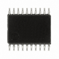
R5F211B1SP#U0 Renesas Electronics America, R5F211B1SP#U0 Datasheet - Page 5

R5F211B1SP#U0
Manufacturer Part Number
R5F211B1SP#U0
Description
IC R8C MCU FLASH 4K 20SSOP
Manufacturer
Renesas Electronics America
Series
M16C™ M16C/R8C/Tiny/1Br
Datasheets
1.R5F211A2SPU0.pdf
(51 pages)
2.R5F211A2SPU0.pdf
(300 pages)
3.R5F211A2SPU0.pdf
(341 pages)
Specifications of R5F211B1SP#U0
Core Processor
R8C
Core Size
16-Bit
Speed
20MHz
Connectivity
I²C, SIO, SSU, UART/USART
Peripherals
LED, POR, Voltage Detect, WDT
Number Of I /o
13
Program Memory Size
4KB (4K x 8)
Program Memory Type
FLASH
Ram Size
384 x 8
Voltage - Supply (vcc/vdd)
2.7 V ~ 5.5 V
Data Converters
A/D 4x10b
Oscillator Type
Internal
Operating Temperature
-20°C ~ 85°C
Package / Case
20-SSOP
For Use With
R0K5211B4S001BE - KIT STARTER FOR R8C/18191A1BR0K5211B4S000BE - KIT DEV EVALUATION R8C/1BR0E521174CPE10 - EMULATOR COMPACT R8C/18/19/1
Lead Free Status / RoHS Status
Lead free / RoHS Compliant
Eeprom Size
-
Available stocks
Company
Part Number
Manufacturer
Quantity
Price
R8C/1A Group, R8C/1B Group
Rev.1.40
REJ03B0144-0140
Table 1.2
NOTE:
CPU
Peripheral
Functions
Electric
Characteristics
Flash Memory
Operating Ambient Temperature
Package
1. I
2. Please contact Renesas Technology sales offices for the Y version.
2
C bus is a trademark of Koninklijke Philips Electronics N. V.
Dec 08, 2006
Functions and Specifications for R8C/1B Group
Number of fundamental
instructions
Minimum instruction execution
time
Operating mode
Address space
Memory capacity
Ports
LED drive ports
Timers
Serial interfaces
Clock synchronous serial interface 1 channel
A/D converter
Watchdog timer
Interrupts
Clock generation circuits
Oscillation stop detection function Main clock oscillation stop detection function
Voltage detection circuit
Power on reset circuit
Supply voltage
Current consumption
Programming and erasure voltage VCC = 2.7 to 5.5 V
Programming and erasure
endurance
Item
Page 3 of 45
89 instructions
50 ns (f(XIN) = 20 MHz, VCC = 3.0 to 5.5 V)
100 ns (f(XIN) = 10 MHz, VCC = 2.7 to 5.5 V)
Single-chip
1 Mbyte
See Table 1.4 Product Information for R8C/1B Group
I/O ports: 13 pins (including LED drive port)
Input port: 3 pins
I/O ports: 4 pins
Timer X: 8 bits × 1 channel, timer Z: 8 bits × 1 channel
(Each timer equipped with 8-bit prescaler)
Timer C: 16 bits × 1 channel
(Input capture and output compare circuits)
1 channel
1 channel
10-bit A/D converter: 1 circuit, 4 channels
15 bits × 1 channel (with prescaler)
Internal: 11 sources, External: 4 sources, Software: 4 sources,
Priority levels: 7 levels
2 circuits
On-chip
On-chip
VCC = 3.0 to 5.5 V (f(XIN) = 20 MHz)
VCC = 2.7 to 5.5 V (f(XIN) = 10 MHz)
Typ. 9 mA (VCC = 5.0 V, f(XIN) = 20 MHz, A/D converter stopped)
Typ. 5 mA (VCC = 3.0 V, f(XIN) = 10 MHz, A/D converter stopped)
Typ. 35 µA (VCC = 3.0 V, wait mode, peripheral clock off)
Typ. 0.7 µA (VCC = 3.0 V, stop mode)
10,000 times (data flash)
1,000 times (program ROM)
-20 to 85°C
-40 to 85°C (D version)
-20 to 105°C (Y version)
20-pin molded-plastic LSSOP
20-pin molded-plastic SDIP
28-pin molded-plastic HWQFN
• Main clock generation circuit (with on-chip feedback
• On-chip oscillator (high speed, low speed)
Reset start selectable, count source protection mode
High-speed on-chip oscillator has a frequency adjustment
function
Clock synchronous serial I/O, UART
UART
I
Clock synchronous serial I/O with chip select (SSU)
2
resistor)
C bus Interface
(1)
Specification
(2)
1. Overview


