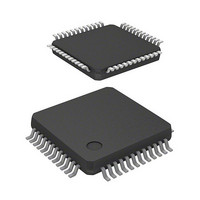
HD64F3672FY Renesas Electronics America, HD64F3672FY Datasheet - Page 148

HD64F3672FY
Manufacturer Part Number
HD64F3672FY
Description
IC H8 MCU FLASH 16K 48QFP
Manufacturer
Renesas Electronics America
Series
H8® H8/300H Tinyr
Datasheet
1.HD64F3672FXV.pdf
(334 pages)
Specifications of HD64F3672FY
Core Processor
H8/300H
Core Size
16-Bit
Speed
16MHz
Connectivity
SCI
Peripherals
PWM, WDT
Number Of I /o
26
Program Memory Size
16KB (16K x 8)
Program Memory Type
FLASH
Ram Size
2K x 8
Voltage - Supply (vcc/vdd)
3 V ~ 5.5 V
Data Converters
A/D 4x10b
Oscillator Type
Internal
Operating Temperature
-20°C ~ 75°C
Package / Case
48-QFP
Lead Free Status / RoHS Status
Contains lead / RoHS non-compliant
Eeprom Size
-
Available stocks
Company
Part Number
Manufacturer
Quantity
Price
Company:
Part Number:
HD64F3672FY
Manufacturer:
Renesas Electronics America
Quantity:
10 000
Company:
Part Number:
HD64F3672FYV
Manufacturer:
Renesas Electronics America
Quantity:
10 000
- Current page: 148 of 334
- Download datasheet (2Mb)
Section 10 Timer V
10.4
10.4.1
1. According to table 10.2, six internal/external clock signals output by prescaler S can be
2. When TCNTV overflows (changes from H'FF to H'00), the overflow flag (OVF) in TCRV0
3. TCNTV is constantly compared with TCORA and TCORB. Compare match flag A or B
4. When a compare match A or B is generated, the TMOV responds with the output value
5. When CCLR1 or CCLR0 in TCRV0 is 01 or 10, TCNTV can be cleared by the corresponding
6. When CCLR1 or CCLR0 in TCRV0 is 11, TCNTV can be cleared by the rising edge of the
7. When a counter-clearing source is generated with TRGE in TCRV1 set to 1, the counting-up is
Rev.4.00 Nov. 02, 2005 Page 122 of 304
REJ09B0143-0400
selected as the timer V operating clock signals. When the operating clock signal is selected,
TCNTV starts counting-up. Figure 10.2 shows the count timing with an internal clock signal
selected, and figure 10.3 shows the count timing with both edges of an external clock signal
selected.
will be set. The timing at this time is shown in figure 10.4. An interrupt request is sent to the
CPU when OVIE in TCRV0 is 1.
(CMFA or CMFB) is set to 1 when TCNTV matches TCORA or TCORB, respectively. The
compare-match signal is generated in the last state in which the values match. Figure 10.5
shows the timing. An interrupt request is generated for the CPU when CMIEA or CMIEB in
TCRV0 is 1.
selected by bits OS3 to OS0 in TCSRV. Figure 10.6 shows the timing when the output is
toggled by compare match A.
compare match. Figure 10.7 shows the timing.
input of TMRIV pin. A TMRIV input pulse-width of at least 1.5 system clocks is necessary.
Figure 10.8 shows the timing.
halted as soon as TCNTV is cleared. TCNTV resumes counting-up when the edge selected by
TVEG1 or TVEG0 in TCRV1 is input from the TGRV pin.
Operation
Timer V Operation
Related parts for HD64F3672FY
Image
Part Number
Description
Manufacturer
Datasheet
Request
R

Part Number:
Description:
(HD64 Series) Hitachi Single-Chip Microcomputer
Manufacturer:
Hitachi Semiconductor
Datasheet:

Part Number:
Description:
KIT STARTER FOR M16C/29
Manufacturer:
Renesas Electronics America
Datasheet:

Part Number:
Description:
KIT STARTER FOR R8C/2D
Manufacturer:
Renesas Electronics America
Datasheet:

Part Number:
Description:
R0K33062P STARTER KIT
Manufacturer:
Renesas Electronics America
Datasheet:

Part Number:
Description:
KIT STARTER FOR R8C/23 E8A
Manufacturer:
Renesas Electronics America
Datasheet:

Part Number:
Description:
KIT STARTER FOR R8C/25
Manufacturer:
Renesas Electronics America
Datasheet:

Part Number:
Description:
KIT STARTER H8S2456 SHARPE DSPLY
Manufacturer:
Renesas Electronics America
Datasheet:

Part Number:
Description:
KIT STARTER FOR R8C38C
Manufacturer:
Renesas Electronics America
Datasheet:

Part Number:
Description:
KIT STARTER FOR R8C35C
Manufacturer:
Renesas Electronics America
Datasheet:

Part Number:
Description:
KIT STARTER FOR R8CL3AC+LCD APPS
Manufacturer:
Renesas Electronics America
Datasheet:

Part Number:
Description:
KIT STARTER FOR RX610
Manufacturer:
Renesas Electronics America
Datasheet:

Part Number:
Description:
KIT STARTER FOR R32C/118
Manufacturer:
Renesas Electronics America
Datasheet:

Part Number:
Description:
KIT DEV RSK-R8C/26-29
Manufacturer:
Renesas Electronics America
Datasheet:

Part Number:
Description:
KIT STARTER FOR SH7124
Manufacturer:
Renesas Electronics America
Datasheet:

Part Number:
Description:
KIT STARTER FOR H8SX/1622
Manufacturer:
Renesas Electronics America
Datasheet:


