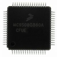
MC9S08GB60ACFUE Freescale Semiconductor, MC9S08GB60ACFUE Datasheet - Page 56

MC9S08GB60ACFUE
Manufacturer Part Number
MC9S08GB60ACFUE
Description
IC MCU 60K FLASH 4K RAM 64-LQFP
Manufacturer
Freescale Semiconductor
Series
HCS08r
Datasheet
1.MC9S08GT60ACFDER.pdf
(302 pages)
Specifications of MC9S08GB60ACFUE
Core Processor
HCS08
Core Size
8-Bit
Speed
40MHz
Connectivity
I²C, SCI, SPI
Peripherals
LVD, POR, PWM, WDT
Number Of I /o
56
Program Memory Size
60KB (60K x 8)
Program Memory Type
FLASH
Ram Size
4K x 8
Voltage - Supply (vcc/vdd)
1.8 V ~ 3.6 V
Data Converters
A/D 8x10b
Oscillator Type
Internal
Operating Temperature
-40°C ~ 85°C
Package / Case
64-LQFP
Processor Series
S08GB
Core
HCS08
Data Bus Width
8 bit
Data Ram Size
4 KB
Interface Type
SCI/SPI
Maximum Clock Frequency
40 MHz
Number Of Programmable I/os
56
Number Of Timers
8
Operating Supply Voltage
0 V to 1.8 V
Maximum Operating Temperature
+ 85 C
Mounting Style
SMD/SMT
3rd Party Development Tools
EWS08
Development Tools By Supplier
M68EVB908GB60E, M68DEMO908GB60E
Minimum Operating Temperature
- 40 C
On-chip Adc
8-ch x 10-bit
For Use With
M68DEMO908GB60E - BOARD DEMO MC9S08GB60M68EVB908GB60E - BOARD EVAL FOR MC9S08GB60
Lead Free Status / RoHS Status
Lead free / RoHS Compliant
Eeprom Size
-
Lead Free Status / Rohs Status
Lead free / RoHS Compliant
Available stocks
Company
Part Number
Manufacturer
Quantity
Price
Company:
Part Number:
MC9S08GB60ACFUE
Manufacturer:
EM
Quantity:
12 000
Company:
Part Number:
MC9S08GB60ACFUE
Manufacturer:
FREESCAL
Quantity:
1 045
Company:
Part Number:
MC9S08GB60ACFUE
Manufacturer:
Freescale Semiconductor
Quantity:
10 000
Part Number:
MC9S08GB60ACFUE
Manufacturer:
FREESCALE
Quantity:
20 000
Company:
Part Number:
MC9S08GB60ACFUER
Manufacturer:
Freescale Semiconductor
Quantity:
10 000
Chapter 4 Memory
4.4.7
Whenever any block protection is enabled, the reset and interrupt vectors will be protected. Vector
redirection allows users to modify interrupt vector information without unprotecting bootloader and reset
vector space. Vector redirection is enabled by programming the FNORED bit in the NVOPT register
located at address 0xFFBF to zero. For redirection to occur, at least some portion but not all of the flash
memory must be block protected by programming the NVPROT register located at address 0xFFBD. All
of the interrupt vectors (memory locations 0xFFC0–0xFFFD) are redirected, while the reset vector
(0xFFFE:FFFF) is not. When more than 32K is protected, vector redirection must not be enabled.
For example, if 512 bytes of flash are protected, the protected address region is from 0xFE00 through
0xFFFF. The interrupt vectors (0xFFC0–0xFFFD) are redirected to the locations 0xFDC0–0xFDFD. Now,
if an SPI interrupt is taken for instance, the values in the locations 0xFDE0:FDE1 are used for the vector
instead of the values in the locations 0xFFE0:FFE1. This allows the user to reprogram the unprotected
portion of the flash with new program code including new interrupt vector values while leaving the
protected area, which includes the default vector locations, unchanged.
4.5
The MC9S08GBxxA/GTxxA includes circuitry to prevent unauthorized access to the contents of flash and
RAM memory. When security is engaged, flash and RAM are considered secure resources. Direct-page
registers, high-page registers, and the background debug controller are considered unsecured resources.
Programs executing within secure memory have normal access to any MCU memory locations and
resources. Attempts to access a secure memory location with a program executing from an unsecured
memory space or through the background debug interface are blocked (writes are ignored and reads return
all 0s).
Security is engaged or disengaged based on the state of two nonvolatile register bits (SEC01:SEC00) in
the FOPT register. During reset, the contents of the nonvolatile location NVOPT are copied from flash into
the working FOPT register in high-page register space. A user engages security by programming the
NVOPT location which can be done at the same time the flash memory is programmed. The 1:0 state
disengages security while the other three combinations engage security. Notice the erased state (1:1) makes
the MCU secure. During development, whenever the flash is erased, it is good practice to immediately
program the SEC00 bit to 0 in NVOPT so SEC01:SEC00 = 1:0. This would allow the MCU to remain
unsecured after a subsequent reset.
The on-chip debug module cannot be enabled while the MCU is secure. The separate background debug
controller can still be used for background memory access commands, but the MCU cannot enter active
background mode except by holding BKGD/MS low at the rising edge of reset.
A user can choose to allow or disallow a security unlocking mechanism through an 8-byte backdoor
security key. If the nonvolatile KEYEN bit in NVOPT/FOPT is 0, the backdoor key is disabled and there
is no way to disengage security without completely erasing all flash locations. If KEYEN is 1, a secure
user program can temporarily disengage security by:
56
1. Writing 1 to KEYACC in the FCNFG register. This makes the flash module interpret writes to the
backdoor comparison key locations (NVBACKKEY through NVBACKKEY+7) as values to be
compared against the key rather than as the first step in a flash program or erase command.
Security
Vector Redirection
MC9S08GB60A Data Sheet, Rev. 2
Freescale Semiconductor


