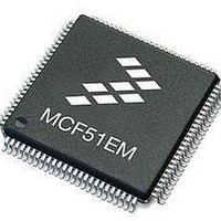
MCF51EM128CLK Freescale Semiconductor, MCF51EM128CLK Datasheet - Page 309

MCF51EM128CLK
Manufacturer Part Number
MCF51EM128CLK
Description
IC MCU 32BIT 128KB FLASH 80LQFP
Manufacturer
Freescale Semiconductor
Series
MCF51EMr
Datasheets
1.MCF51EM128CLL.pdf
(2 pages)
2.MCF51EM128CLL.pdf
(54 pages)
3.MCF51EM128CLL.pdf
(636 pages)
Specifications of MCF51EM128CLK
Core Processor
Coldfire V1
Core Size
32-Bit
Speed
50MHz
Connectivity
I²C, SCI, SPI
Peripherals
LCD, LVD, PWM, WDT
Number Of I /o
56
Program Memory Size
128KB (128K x 8)
Program Memory Type
FLASH
Ram Size
8K x 8
Voltage - Supply (vcc/vdd)
1.8 V ~ 3.6 V
Data Converters
A/D 12x16b
Oscillator Type
External
Operating Temperature
-40°C ~ 85°C
Package / Case
80-LQFP
Processor Series
MCF51EM
Core
ColdFire V1
Data Bus Width
32 bit
Data Ram Size
16 KB
Interface Type
RS-232, LIN
Maximum Clock Frequency
50 MHz
Number Of Timers
3
Operating Supply Voltage
1.8 V to 3.6 V
Maximum Operating Temperature
+ 85 C
Mounting Style
SMD/SMT
3rd Party Development Tools
JLINK-CF-BDM26, EWCF
Development Tools By Supplier
TWR-MCF51CN-KIT, TWR-SER, TWR-ELEV, TOWER
Minimum Operating Temperature
- 40 C
Lead Free Status / RoHS Status
Lead free / RoHS Compliant
Eeprom Size
-
Lead Free Status / Rohs Status
Details
Available stocks
Company
Part Number
Manufacturer
Quantity
Price
Company:
Part Number:
MCF51EM128CLK
Manufacturer:
Freescale Semiconductor
Quantity:
10 000
- Current page: 309 of 636
- Download datasheet (11Mb)
MOSI input of a slave or the MISO input of a master. The MOSI waveform applies to the MOSI output
pin from a master and the MISO waveform applies to the MISO output from a slave. The SS OUT
waveform applies to the slave select output from a master (provided MODFEN and SSOE = 1). The master
SS output goes to active low at the start of the first bit time of the transfer and goes back high one-half
SPSCK cycle after the end of the eighth bit time of the transfer. The SS IN waveform applies to the slave
select input of a slave.
When CPHA = 0, the slave begins to drive its MISO output with the first data bit value (MSB or LSB
depending on LSBFE) when SS goes to active low. The first SPSCK edge causes both the master and the
slave to sample the data bit values on their MISO and MOSI inputs, respectively. At the second SPSCK
edge, the SPI shifter shifts one bit position which shifts in the bit value that was just sampled and shifts the
second data bit value out the other end of the shifter to the MOSI and MISO outputs of the master and
slave, respectively. When CPHA = 0, the slave’s SS input must go to its inactive high level between
transfers.
13.4.7
As shown in
prescale bits (SPPR2:SPPR1:SPPR0) choose a prescale divisor of 1, 2, 3, 4, 5, 6, 7, or 8. The three rate
Freescale Semiconductor
(MISO OR MOSI)
(MASTER OUT)
(REFERENCE)
(SLAVE OUT)
SAMPLE IN
MSB FIRST
BIT TIME #
(CPOL = 0)
(CPOL = 1)
LSB FIRST
(MASTER)
(SLAVE)
SS OUT
SPSCK
SPSCK
SS IN
MOSI
MISO
SPI Baud Rate Generation
Figure
MCF51EM256 Series ColdFire Integrated Microcontroller Reference Manual, Rev. 8
13-18, the clock source for the SPI baud rate generator is the bus clock. The three
BIT 7
BIT 0
1
Figure 13-17. SPI Clock Formats (CPHA = 0)
BIT 6
BIT 1
2
...
...
...
BIT 2
BIT 5
6
BIT 1
BIT 6
7
16-Bit Serial Peripheral Interface (SPI16)
BIT 0
BIT 7
8
13-23
Related parts for MCF51EM128CLK
Image
Part Number
Description
Manufacturer
Datasheet
Request
R

Part Number:
Description:
IC MCU 32BIT 256KB FLASH 100LQFP
Manufacturer:
Freescale Semiconductor
Datasheet:

Part Number:
Description:
BOARD DEMO HARDWARE ONLY
Manufacturer:
Freescale Semiconductor
Datasheet:

Part Number:
Description:
IC MCU 32BIT 128KB FLASH 100LQFP
Manufacturer:
Freescale Semiconductor
Datasheet:

Part Number:
Description:
IC MCU 32BIT 256KB FLASH 80LQFP
Manufacturer:
Freescale Semiconductor
Datasheet:
Part Number:
Description:
Manufacturer:
Freescale Semiconductor, Inc
Datasheet:
Part Number:
Description:
Manufacturer:
Freescale Semiconductor, Inc
Datasheet:
Part Number:
Description:
Manufacturer:
Freescale Semiconductor, Inc
Datasheet:
Part Number:
Description:
Manufacturer:
Freescale Semiconductor, Inc
Datasheet:
Part Number:
Description:
Manufacturer:
Freescale Semiconductor, Inc
Datasheet:
Part Number:
Description:
Manufacturer:
Freescale Semiconductor, Inc
Datasheet:
Part Number:
Description:
Manufacturer:
Freescale Semiconductor, Inc
Datasheet:
Part Number:
Description:
Manufacturer:
Freescale Semiconductor, Inc
Datasheet:
Part Number:
Description:
Manufacturer:
Freescale Semiconductor, Inc
Datasheet:
Part Number:
Description:
Manufacturer:
Freescale Semiconductor, Inc
Datasheet:


