M30280F6HP#U7B Renesas Electronics America, M30280F6HP#U7B Datasheet - Page 150
M30280F6HP#U7B
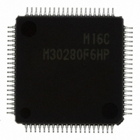
Manufacturer Part Number
M30280F6HP#U7B
Description
IC M16C/28 MCU FLASH 80LQFP
Manufacturer
Renesas Electronics America
Series
M16C™ M16C/Tiny/28r
Datasheet
1.M30280F6HPU9.pdf
(425 pages)
Specifications of M30280F6HP#U7B
Core Processor
M16C/60
Core Size
16-Bit
Speed
20MHz
Connectivity
I²C, IEBus, SIO, UART/USART
Peripherals
DMA, POR, PWM, Voltage Detect, WDT
Number Of I /o
71
Program Memory Size
48KB (48K x 8)
Program Memory Type
FLASH
Ram Size
4K x 8
Voltage - Supply (vcc/vdd)
2.7 V ~ 5.5 V
Data Converters
A/D 24x10b
Oscillator Type
Internal
Operating Temperature
-40°C ~ 85°C
Package / Case
80-LQFP
For Use With
R0K330290S000BE - KIT EVAL STARTER FOR M16C/29M30290T2-CPE - EMULATOR COMPACT M16C/26A/28/29M30290T2-CPE-HP - EMULATOR COMPACT FOR M16C/TINY
Lead Free Status / RoHS Status
Lead free / RoHS Compliant
Eeprom Size
-
Available stocks
Company
Part Number
Manufacturer
Quantity
Price


M
R
R
e
E
1
Figure 12.30 TB2SC Register
. v
J
6
0
C
2
9
2 /
0 .
B
Timer B2 Special Mode Register
0
8
b7
0
0
NOTES:
G
4
J
0
b6
1. Write to this register after setting the PRC1 bit in the PRCR register to 1 (write enabled).
2. If the INV11 bit is 0 (three-phase mode 0) or the INV06 bit is 1 (triangular wave modulation mode), set this bit to 0 (timer
3. When setting the IVPCR1 bit to 1 (three-phase output forcible cutoff by SD pin input enabled), Set the PD8
4. Related pins are U(P8
5. When this bit is used in delayed trigger mode 0, set bits TB0EN and TB1EN to 1 (A/D trigger mode).
6. When setting the TB2SEL bit to 1 (underflow of TB2 interrupt generation frequency setting counter[ICTB2]), set the INV02
NOTES:
2.Case of INV03 = 0(Three-phase motor control timer output disabled)
NOTE:
The effect of SD pin input is below.
1.Case of INV03 = 1(Three-phase motor control timer output enabled)
7
forcrible cutoff disable)
a
forcrible cutoff disable)
forcrible cutoff enable)
forcrible cutoff enable)
o r
(Three-phase output
(Three-phase output
(Three-phase output
(Three-phase output
0 -
B2 underflow).
mode).
and set the IVPCR1 bit to 0 after forcible cutoff, pins U, U, V, V, W, and W are exit from the high-impedance state. If a low-
level (“L”) signal is applied to the SD pin, three-phase motor control timer output will be disabled (INV03=0). At this time,
when the IVPCR1 bit is 0, pins U, U, V, V, W, and W become programmable I/O ports. When the IVPCR1 bit is set to 1,
pins U, U, V, V, W, and W are placed in a high-impedance state regardless of which function of those pins is used.
bit to 1 (three-phase motor control timer function).
. n
1. When "L" is applied to the SD pin, INV03 bit is changed to 0 at the same time.
2. The value of the port register and the port direction register becomes effective.
3. When SD function is not used, set to 0 (Input) in PD8
4. To leave the high-impedance state and restart the three-phase PWM signal output after the three-phase PWM signal
0
1. The three-phase output forcrible cutoff function becomes effective if the INPCR1 bit is set to 1 (three-phase output
b5
u
2
output forced cutoff, set the IVPCR1 bit to 0 after the SD pin input level becomes high (“H”).
3
p
forcrible cutoff function enable) even when the INV03 bit is 0 (three-phase motor control timer output disalbe)
0
IVPCR1 bit
IVPCR1 bit
b4
, 1
0
(
M
2
b3
1
0
1
0
0
1
0
6
b2
7
C
b1
2 /
page 128
, 8
b0
M
0
Bit Symbol
), U(P8
PWCON
IVPCR1
TB2SEL
(b6-b5)
TB0EN
1
TB1EN
6
(b7)
Symbol
TB2SC
C
SD pin inputs
SD pin inputs
2 /
1
f o
), V(P7
8
3
) B
Timer B0 operation mode
select bit
Three-phase output port
SD control bit 1
Timer B1 operation mode
select bit
H
H
Timer B2 reload timing
switch bit
L
L
8
Trigger select bit
H
H
L
Reserved bits
L
Nothing is assigned. If necessary, set to 0.
When read, the content is 0.
5
(1)
(1)
(1)
2
), V(P7
Address
039E
(3)
Bit Name
3
(2)
16
), W(P7
(3, 4, 7)
Three-phase PWM output
Three-phase PWM output
(6)
Peripheral input/output
Peripheral input/output
Peripheral input/output
4
Status of U/V/W pins
Status of U/V/W pins
), W(P7
5
or input/output port
or input/output port
or input/output port
Input/output port
and pullup to "H" in SD pin from outside.
High impedance
High impedance
0: Timer B2 underflow
1: Timer A output at odd-numbered
0: Three-phase output forcible cutoff by SD pin input
1: Three-phase output forcible cutoff by SD pin input
0: TB2 interrupt
1: Underflow of TB2 interrupt
0: Other than A/D trigger mode
1: A/D trigger mode
0: Other than A/D trigger mode
1: A/D trigger mode
5
After Reset
X0000000
Set to 0
). When a high-level ("H") signal is applied to the SD pin
(high impedance) disabled
(high impedance) enabled
generation frequency setting counter [ICTB2]
(2)
2
(4)
Function
Three-phase output
forcrible cutoff
Three-phase output
forcrible cutoff
(5)
(5)
Remarks
Remarks
(1)
5
bit to 0 (= input
RW
RW
RW
RW
RW
RW
RW
12. Timer
Related parts for M30280F6HP#U7B
Image
Part Number
Description
Manufacturer
Datasheet
Request
R

Part Number:
Description:
KIT STARTER FOR M16C/29
Manufacturer:
Renesas Electronics America
Datasheet:

Part Number:
Description:
KIT STARTER FOR R8C/2D
Manufacturer:
Renesas Electronics America
Datasheet:

Part Number:
Description:
R0K33062P STARTER KIT
Manufacturer:
Renesas Electronics America
Datasheet:

Part Number:
Description:
KIT STARTER FOR R8C/23 E8A
Manufacturer:
Renesas Electronics America
Datasheet:

Part Number:
Description:
KIT STARTER FOR R8C/25
Manufacturer:
Renesas Electronics America
Datasheet:

Part Number:
Description:
KIT STARTER H8S2456 SHARPE DSPLY
Manufacturer:
Renesas Electronics America
Datasheet:

Part Number:
Description:
KIT STARTER FOR R8C38C
Manufacturer:
Renesas Electronics America
Datasheet:

Part Number:
Description:
KIT STARTER FOR R8C35C
Manufacturer:
Renesas Electronics America
Datasheet:

Part Number:
Description:
KIT STARTER FOR R8CL3AC+LCD APPS
Manufacturer:
Renesas Electronics America
Datasheet:
Part Number:
Description:
KIT STARTER FOR RX610
Manufacturer:
Renesas Electronics America
Datasheet:

Part Number:
Description:
KIT STARTER FOR R32C/118
Manufacturer:
Renesas Electronics America
Datasheet:

Part Number:
Description:
KIT DEV RSK-R8C/26-29
Manufacturer:
Renesas Electronics America
Datasheet:

Part Number:
Description:
KIT STARTER FOR SH7124
Manufacturer:
Renesas Electronics America
Datasheet:

Part Number:
Description:
KIT STARTER FOR H8SX/1622
Manufacturer:
Renesas Electronics America
Datasheet:

Part Number:
Description:
KIT DEV FOR SH7203
Manufacturer:
Renesas Electronics America
Datasheet: