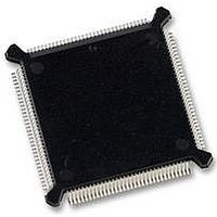
MC68331CEH25 Freescale Semiconductor, MC68331CEH25 Datasheet - Page 29

MC68331CEH25
Manufacturer Part Number
MC68331CEH25
Description
IC MCU 32BIT 25MHZ 132-PQFP
Manufacturer
Freescale Semiconductor
Series
M683xxr
Specifications of MC68331CEH25
Core Processor
CPU32
Core Size
32-Bit
Speed
25MHz
Connectivity
EBI/EMI, SCI, SPI, UART/USART
Peripherals
POR, PWM, WDT
Number Of I /o
18
Program Memory Type
ROMless
Voltage - Supply (vcc/vdd)
4.5 V ~ 5.5 V
Oscillator Type
Internal
Operating Temperature
-40°C ~ 85°C
Package / Case
132-QFP
Controller Family/series
68K
No. Of I/o's
18
Cpu Speed
25MHz
No. Of Timers
1
Embedded Interface Type
QSPI, SCI, UART
No. Of Pwm Channels
2
Digital Ic Case Style
PQFP
Rohs Compliant
Yes
Processor Series
M683xx
Core
CPU32
Data Bus Width
32 bit
Data Ram Size
80 B
Interface Type
QSPI, SCI, UART
Maximum Clock Frequency
25 MHz
Number Of Programmable I/os
18
Number Of Timers
1
Maximum Operating Temperature
+ 85 C
Mounting Style
SMD/SMT
Minimum Operating Temperature
- 40 C
Eeprom Size
-
Ram Size
-
Program Memory Size
-
Data Converters
-
Lead Free Status / Rohs Status
Details
Available stocks
Company
Part Number
Manufacturer
Quantity
Price
Company:
Part Number:
MC68331CEH25
Manufacturer:
PANASONIC
Quantity:
2 000
Company:
Part Number:
MC68331CEH25
Manufacturer:
Freescale Semiconductor
Quantity:
135
Company:
Part Number:
MC68331CEH25
Manufacturer:
Freescale Semiconductor
Quantity:
10 000
3.5.1 Chip-Select Registers
MC68331TS/D
The following table lists allocation of chip-selects and discrete outputs on the pins of the MCU.
Pin assignment registers CSPAR0 and CSPAR1 determine functions of chip-select pins. These regis-
ters also determine port size (8- or 16-bit) for dynamic bus allocation.
A pin data register (PORTC) latches discrete output data.
Blocks of addresses are assigned to each chip-select function. Block sizes of 2 Kbytes to 1 Mbyte can
be selected by writing values to the appropriate base address register (CSBAR). Address blocks for
separate chip-select functions can overlap.
Chip-select option registers (CSORBT and CSOR[10:0]) determine timing of and conditions for asser-
tion of chip-select signals. Eight parameters, including operating mode, access size, synchronization,
and wait state insertion can be specified.
Initialization code often resides in a peripheral memory device controlled by the chip-select circuits. A
set of special chip-select functions and registers (CSORBT, CSBARBT) is provided to support bootstrap
operation.
DSACK
BUS CONTROL
AVEC
ADDRESS
INTERNAL
SIGNALS
Freescale Semiconductor, Inc.
GENERATOR
Figure 9 Chip-Select Circuit Block Diagram
CSBOOT
For More Information On This Product,
ADDR19
ADDR20
ADDR21
ADDR22
ADDR23
BGACK
AVEC
FC0
FC1
FC2
Pin
BR
BG
BASE ADDRESS REGISTER
ADDRESS COMPARATOR
OPTION COMPARE
OPTION REGISTER
Go to: www.freescale.com
GENERATOR
DSACK
Chip Select
CSBOOT
CS10
CS0
CS1
CS2
CS3
CS4
CS5
CS6
CS7
CS8
CS9
ASSIGNMENT
REGISTER
Discrete Outputs
PIN
ECLK
CONTROL
PC0
PC1
PC2
PC3
PC4
PC5
PC6
TIMING
—
—
—
—
AND
REGISTER
DATA
PIN
PIN
CHIP SEL BLOCK
29


