M38513E4FP#U0 Renesas Electronics America, M38513E4FP#U0 Datasheet - Page 34
M38513E4FP#U0
Manufacturer Part Number
M38513E4FP#U0
Description
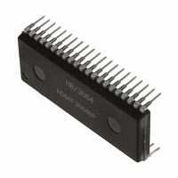
IC 740 MCU ROM 16K 42SSOP
Manufacturer
Renesas Electronics America
Series
740/38000r
Specifications of M38513E4FP#U0
Core Processor
740
Core Size
8-Bit
Speed
8MHz
Connectivity
SIO, UART/USART
Peripherals
PWM, WDT
Number Of I /o
34
Program Memory Size
16KB (16K x 8)
Program Memory Type
OTP
Ram Size
512 x 8
Voltage - Supply (vcc/vdd)
2.7 V ~ 5.5 V
Data Converters
A/D 5x10b
Oscillator Type
External
Operating Temperature
-20°C ~ 85°C
Package / Case
42-SSOP
Package
42SSOP
Family Name
740
Maximum Speed
8 MHz
Operating Supply Voltage
5 V
Data Bus Width
8 Bit
Number Of Programmable I/os
34
Interface Type
I2C-BUS
On-chip Adc
5-chx10-bit
Number Of Timers
4
Lead Free Status / RoHS Status
Contains lead / RoHS non-compliant
Eeprom Size
-


3851 Group
[I
The I
cation format.
•Bits 0 to 2: Bit counter (BC0–BC2)
These bits decide the number of bits for the next 1-byte data to be
transmitted. The I
after the number of count specified with these bits (ACK clock is
added to the number of count when ACK clock is selected by ACK
clock bit (bit 7 of address 002F
BC0 to BC2 are returned to “000
Also when a START condition is received, these bits become
“000
8 bits.
•Bit 3: I
This bit enables to use the multi-master I
this bit is set to “0”, the use disable status is provided, so that the
SDA and the SCL become high-impedance. When the bit is set to
“1”, use of the interface is enabled.
When ES0 = “0”, the following is performed.
• PIN = “1”, BB = “0” and AL = “0” are set (which are bits of the I
• Writing data to the I
•Bit 4: Data format selection bit (ALS)
This bit decides whether or not to recognize slave addresses.
When this bit is set to “0”, the addressing format is selected, so
that address data is recognized. When a match is found between
a slave address and address data as a result of comparison or
when a general call (refer to “I
ceived, transfer processing can be performed. When this bit is set
to “1”, the free data format is selected, so that slave addresses are
not recognized.
•Bit 5: Addressing format selection bit (10BIT SAD)
This bit selects a slave address specification format. When this bit
is set to “0”, the 7-bit addressing format is selected. In this case,
only the high-order 7 bits (slave address) of the I
ter (address 002C
bit is set to “1”, the 10-bit addressing format is selected, and all
the bits of the I
data.
•Bit 6: SDA/SCL pin selection bit (TSEL)
This bit selects the input/output pins of SCL and SDA of the multi-
master I
•Bit 7: I
This bit selects the input level of the SCL and SDA pins of the
multi-master I
Rev.1.01
status register at address 002D
abled.
2
C Control Register (S1D)] 002E
2
2
” and the address data is always transmitted and received in
C control register (address 002E
2
2
2
C interface enable bit (ES0)
C-BUS interface pin input level selection bit (TISS)
C-BUS interface.
Oct 15, 2003
2
C-BUS interface.
(Built-in 24 KB or more ROM)
2
C address register are compared with address
2
16
C interrupt request signal occurs immediately
) are compared with address data. When this
2
C data shift register (address 002B
page 32 of 89
2
2
16
16
C Status Register”, bit 1) is re-
”.
)) have been transferred, and
).
16
) controls data communi-
2
C-BUS interface. When
16
2
C address regis-
16
) is dis-
2
C
Fig. 30 SDA/SCL pin selection bit
Fig. 31 Structure of I
TISS TSEL
b7
Multi-master
I C-BUS interface
2
10 BIT
SAD
ALS ES0 BC2 BC1 BC0
S D A
S C L
2
C control register
T S E L
T S E L
T S E L
T S E L
b0
I
(S1D : address 002E
Bit counter (Number of
transmit/receive bits)
I
enable bit
Data format selection bit
Addressing format
selection bit
SDA/SCL pin selection bit
I
level selection bit
2
2
2
C control register
C-BUS interface
C-BUS interface pin input
b2 b1 b0
0
0
0
0
1
1
1
1
0 : Disabled
1 : Enabled
0 : Addressing format
1 : Free data format
0 : 7-bit addressing
1 : 10-bit addressing
0 : Connect to ports P2
1 : Connect to ports P2
0 : CMOS input
1 : SMBUS input
format
format
0
0
1
1
0
0
1
1
0 : 8
1 : 7
0 : 6
1 : 5
0 : 4
1 : 3
0 : 2
1 : 1
S C L
S C L
S D A
S D A
1
2
1
2
/ P 2
/ T x D / P 2
/ P 2
/ R x D / P 2
3
2
16
)
5
4
2
4
, P2
, P2
3
5
Related parts for M38513E4FP#U0
Image
Part Number
Description
Manufacturer
Datasheet
Request
R

Part Number:
Description:
KIT STARTER FOR M16C/29
Manufacturer:
Renesas Electronics America
Datasheet:

Part Number:
Description:
KIT STARTER FOR R8C/2D
Manufacturer:
Renesas Electronics America
Datasheet:

Part Number:
Description:
R0K33062P STARTER KIT
Manufacturer:
Renesas Electronics America
Datasheet:

Part Number:
Description:
KIT STARTER FOR R8C/23 E8A
Manufacturer:
Renesas Electronics America
Datasheet:

Part Number:
Description:
KIT STARTER FOR R8C/25
Manufacturer:
Renesas Electronics America
Datasheet:

Part Number:
Description:
KIT STARTER H8S2456 SHARPE DSPLY
Manufacturer:
Renesas Electronics America
Datasheet:

Part Number:
Description:
KIT STARTER FOR R8C38C
Manufacturer:
Renesas Electronics America
Datasheet:

Part Number:
Description:
KIT STARTER FOR R8C35C
Manufacturer:
Renesas Electronics America
Datasheet:

Part Number:
Description:
KIT STARTER FOR R8CL3AC+LCD APPS
Manufacturer:
Renesas Electronics America
Datasheet:
Part Number:
Description:
KIT STARTER FOR RX610
Manufacturer:
Renesas Electronics America
Datasheet:

Part Number:
Description:
KIT STARTER FOR R32C/118
Manufacturer:
Renesas Electronics America
Datasheet:

Part Number:
Description:
KIT DEV RSK-R8C/26-29
Manufacturer:
Renesas Electronics America
Datasheet:

Part Number:
Description:
KIT STARTER FOR SH7124
Manufacturer:
Renesas Electronics America
Datasheet:

Part Number:
Description:
KIT STARTER FOR H8SX/1622
Manufacturer:
Renesas Electronics America
Datasheet:

Part Number:
Description:
KIT DEV FOR SH7203
Manufacturer:
Renesas Electronics America
Datasheet: