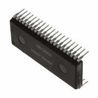
M38513E4FP#U0 Renesas Electronics America, M38513E4FP#U0 Datasheet - Page 64

M38513E4FP#U0
Manufacturer Part Number
M38513E4FP#U0
Description
IC 740 MCU ROM 16K 42SSOP
Manufacturer
Renesas Electronics America
Series
740/38000r
Specifications of M38513E4FP#U0
Core Processor
740
Core Size
8-Bit
Speed
8MHz
Connectivity
SIO, UART/USART
Peripherals
PWM, WDT
Number Of I /o
34
Program Memory Size
16KB (16K x 8)
Program Memory Type
OTP
Ram Size
512 x 8
Voltage - Supply (vcc/vdd)
2.7 V ~ 5.5 V
Data Converters
A/D 5x10b
Oscillator Type
External
Operating Temperature
-20°C ~ 85°C
Package / Case
42-SSOP
Package
42SSOP
Family Name
740
Maximum Speed
8 MHz
Operating Supply Voltage
5 V
Data Bus Width
8 Bit
Number Of Programmable I/os
34
Interface Type
I2C-BUS
On-chip Adc
5-chx10-bit
Number Of Timers
4
Lead Free Status / RoHS Status
Contains lead / RoHS non-compliant
Eeprom Size
-
3851 Group
Table 18 Description of pin function (Standard Serial I/O Mode)
Rev.1.01
RESET
X
AV
V
P0
P1
V
CNV
X
P2
P2
P2
P2
P2
P3
P4
P4
IN
REF
OUT
CC
0
0
0
4
5
6
7
0
0
1
SS
, P4
,V
to P0
to P1
to P2
to P3
SS
Pin
SS
2
to P4
7
7
3
4
Oct 15, 2003
(Built-in 24 KB or more ROM)
4
Clock input
TxD output
CNV
Reset input
Clock output
Analog power supply input
Reference voltage input
Input port P0
Input port P1
Input port P2
RxD input
BUSY output
Input port P3
Input port P4
Power input
S
Input port P4
CLK1
SS
input
page 62 of 89
Name
I/O
O
O
O
I
I
I
I
I
I
I
I
I
I
I
I
Enter the reference voltage for AD from this pin, or open.
This pin is for BUSY signal output.
Connect a ceramic resonator or crystal oscillator between X
X
and open X
Connect AV
This pin is for serial clock input.
Input “H” when RESET is released only.
Connect to V
Connect to Vpp (=4.5 V to 5.5 V) when V
Reset input pin. While reset is “L” level, a 20 cycle or longer clock
Input “H” or “L”, or open.
Input “H” or “L”, or open.
Input “H” or “L”, or open.
This pin is for serial data input.
This pin is for serial data output.
Input “H” or “L”, or open.
Input “H” or “L”, or open.
Apply program/erase protection voltage to Vcc pin and 0 V to Vss pin.
must be input to X
OUT
pins. To input an externally generated clock, input it to X
OUT
SS
CC
to V
pin.
when V
IN
SS
pin.
.
CC
Description
= 4.5 V to 5.5 V.
CC
= 2.7 V to 4.5 V.
IN
and
IN
pin


