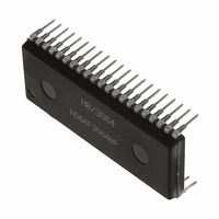
M38513E4FP#U0 Renesas Electronics America, M38513E4FP#U0 Datasheet - Page 38

M38513E4FP#U0
Manufacturer Part Number
M38513E4FP#U0
Description
IC 740 MCU ROM 16K 42SSOP
Manufacturer
Renesas Electronics America
Series
740/38000r
Specifications of M38513E4FP#U0
Core Processor
740
Core Size
8-Bit
Speed
8MHz
Connectivity
SIO, UART/USART
Peripherals
PWM, WDT
Number Of I /o
34
Program Memory Size
16KB (16K x 8)
Program Memory Type
OTP
Ram Size
512 x 8
Voltage - Supply (vcc/vdd)
2.7 V ~ 5.5 V
Data Converters
A/D 5x10b
Oscillator Type
External
Operating Temperature
-20°C ~ 85°C
Package / Case
42-SSOP
Package
42SSOP
Family Name
740
Maximum Speed
8 MHz
Operating Supply Voltage
5 V
Data Bus Width
8 Bit
Number Of Programmable I/os
34
Interface Type
I2C-BUS
On-chip Adc
5-chx10-bit
Number Of Timers
4
Lead Free Status / RoHS Status
Contains lead / RoHS non-compliant
Eeprom Size
-
3851 Group
[I
(S2D)] 0030
The I
controls START/STOP condition detection.
•Bits 0 to 4: START/STOP condition set bit (SSC4–SSC0)
SCL release time, setup time, and hold time change the detection
condition by value of the main clock divide ratio selection bit and
the oscillation frequency f(X
by the internal system clock. Accordingly, set the proper value to
the START/STOP condition set bits (SSC4 to SSC0) in considered
of the system clock frequency. Refer to Table 13.
Do not set “00000
tion set bit (SSC4 to SSC0).
Refer to Table 14, the recommended set value to START/STOP
condition set bits (SSC4–SSC0) for each oscillation frequency.
•Bit 5: SCL/SDA interrupt pin polarity selection bit (SIP)
An interrupt can occur when detecting the falling or rising edge of
the SCL or SDA pin. This bit selects the polarity of the SCL or
SDA pin interrupt pin.
•Bit 6: SCL/SDA interrupt pin selection bit (SIS)
This bit selects the pin of which interrupt becomes valid between
the SCL pin and the SDA pin.
Note: When changing the setting of the SCL/SDA interrupt pin polarity se-
Rev.1.01
2
C START/STOP Condition Control Register
2
lection bit, the SCL/SDA interrupt pin selection bit, or the I
interface enable bit ES0, the SCL/SDA interrupt request bit may be
set. When selecting the SCL/SDA interrupt source, disable the inter-
rupt before the SCL/SDA interrupt pin polarity selection bit, the SCL/
SDA interrupt pin selection bit, or the I
ES0 is set. Reset the request bit to “0” after setting these bits, and
enable the interrupt.
C START/STOP condition control register (address 0030
Oct 15, 2003
(Built-in 24 KB or more ROM)
16
2
” or an odd number to the START/STOP condi-
IN
page 36 of 89
) because these time are measured
2
C-BUS interface enable bit
2
C-BUS
16
)
Address Data Communication
There are two address data communication formats, namely, 7-bit
addressing format and 10-bit addressing format. The respective
address communication formats are described below.
(1) 7-bit addressing format
(2) 10-bit addressing format
To adapt the 7-bit addressing format, set the 10BIT SAD bit of
the I
address data transmitted from the master is compared with the
high-order 7-bit slave address stored in the I
ter (address 002C
comparison of the RWB bit of the I
dress 002C
format when the 7-bit addressing format is selected, refer to
Figure 39, (1) and (2).
To adapt the 10-bit addressing format, set the 10BIT SAD bit of
the I
comparison is performed between the first-byte address data
transmitted from the master and the 8-bit slave address stored
in the I
this comparison, an address comparison between the RWB bit
of the I
which is the last bit of the address data transmitted from the
master is made. In the 10-bit addressing mode, the RWB bit
which is the last bit of the address data not only specifies the
direction of communication for control data, but also is pro-
cessed as an address data bit.
When the first-byte address data agree with the slave address,
the AAS bit of the I
“1”. After the second-byte address data is stored into the I
data shift register (address 002B
parison between the second-byte data and the slave address
by software. When the address data of the 2 bytes agree with
the slave address, set the RWB bit of the I
(address 002C
make the 7-bit slave address and R/W data agree, which are
received after a RESTART condition is detected, with the value
of the I
transmission format when the 10-bit addressing format is se-
lected, refer to Figure 39, (3) and (4).
2
2
C control register (address 002E
C control register (address 002E
2
2
2
C address register (address 002C
C address register (address 002C
C address register (address 002C
16
) is not performed. For the data transmission
16
) to “1” by software. This processing can
16
2
C status register (address 002D
). At the time of this comparison, address
16
), perform an address com-
2
C address register (ad-
16
16
) to “0”. The first 7-bit
) to “1”. An address
2
16
C address register
16
2
16
) and the R/W bit
C address regis-
). At the time of
). For the data
16
) is set to
2
C


