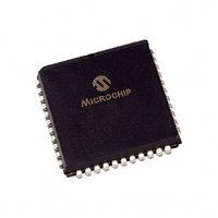
PIC16C774-E/L Microchip Technology, PIC16C774-E/L Datasheet - Page 11

PIC16C774-E/L
Manufacturer Part Number
PIC16C774-E/L
Description
IC MCU OTP 4KX14 A/D PWM 44PLCC
Manufacturer
Microchip Technology
Series
PIC® 16Cr
Datasheets
1.PIC16F616T-ISL.pdf
(8 pages)
2.PIC16C773SO.pdf
(201 pages)
3.PIC16C774P.pdf
(13 pages)
4.PIC16C774P.pdf
(16 pages)
Specifications of PIC16C774-E/L
Core Processor
PIC
Core Size
8-Bit
Speed
20MHz
Connectivity
I²C, SPI, UART/USART
Peripherals
Brown-out Detect/Reset, POR, PWM, WDT
Number Of I /o
33
Program Memory Size
7KB (4K x 14)
Program Memory Type
OTP
Ram Size
256 x 8
Voltage - Supply (vcc/vdd)
4 V ~ 5.5 V
Data Converters
A/D 10x12b
Oscillator Type
External
Operating Temperature
-40°C ~ 125°C
Package / Case
44-PLCC
For Use With
DVA16XL441 - ADAPTER DEVICE ICE 44PLCC
Lead Free Status / RoHS Status
Lead free / RoHS Compliant
Eeprom Size
-
Other names
PIC16C774E/L
Available stocks
Company
Part Number
Manufacturer
Quantity
Price
Company:
Part Number:
PIC16C774-E/L
Manufacturer:
Microchip Technology
Quantity:
10 000
- PIC16F616T-ISL PDF datasheet
- PIC16C773SO PDF datasheet #2
- PIC16C774P PDF datasheet #3
- PIC16C774P PDF datasheet #4
- Current page: 11 of 201
- Download datasheet (3Mb)
2.0
There are two memory blocks in each of these
PICmicro
gram Memory and Data Memory) has its own bus
so that concurrent access can occur.
Additional information on device memory may be found
in the PICmicro
(DS33023).
2.1
The PIC16C77X PICmicros have a 13-bit program
counter capable of addressing an 8K x 14 program
memory space. Each device has 4K x 14 words of pro-
gram memory. Accessing a location above the physi-
cally implemented address will cause a wraparound.
The reset vector is at 0000h and the interrupt vector is
at 0004h.
FIGURE 2-1:
Program
Memory
On-chip
1999 Microchip Technology Inc.
CALL, RETURN
RETFIE, RETLW
MEMORY ORGANIZATION
Program Memory Organization
®
microcontrollers. Each block (Pro-
PROGRAM MEMORY MAP
AND STACK
Interrupt Vector
Mid-Range Reference Manual,
Stack Level 8
Stack Level 2
Stack Level 1
Reset Vector
PC<12:0>
Page 0
Page 1
13
0000h
0004h
0005h
07FFh
0800h
0FFFh
1000h
Advance Information
3FFFh
2.2
The data memory is partitioned into multiple banks
which contain the General Purpose Registers and the
Special Function Registers. Bits RP1 and RP0 are the
bank select bits.
Each bank extends up to 7Fh (128 bytes). The lower
locations of each bank are reserved for the Special
Function Registers. Above the Special Function Regis-
ters are General Purpose Registers, implemented as
static RAM. All implemented banks contain special
function registers. Some “high use” special function
registers from one bank may be mirrored in another
bank for code reduction and quicker access.
2.2.1
The register file can be accessed either directly, or indi-
rectly through the File Select Register FSR.
= 00
= 01
= 10
= 11
RP1
Data Memory Organization
GENERAL PURPOSE REGISTER FILE
RP0
Bank0
Bank1
Bank2
Bank3
(STATUS<6:5>)
PIC16C77X
DS30275A-page 11
Related parts for PIC16C774-E/L
Image
Part Number
Description
Manufacturer
Datasheet
Request
R

Part Number:
Description:
IC MCU OTP 8KX14 A/D PWM 44PLCC
Manufacturer:
Microchip Technology
Datasheet:

Part Number:
Description:
IC MCU OTP 8KX14 A/D PWM 44PLCC
Manufacturer:
Microchip Technology
Datasheet:

Part Number:
Description:
IC MCU OTP 8KX14 A/D PWM 44TQFP
Manufacturer:
Microchip Technology
Datasheet:

Part Number:
Description:
IC MCU OTP 8KX14 A/D PWM 44-MQFP
Manufacturer:
Microchip Technology
Datasheet:

Part Number:
Description:
IC MCU OTP 8KX14 A/D PWM 40DIP
Manufacturer:
Microchip Technology
Datasheet:

Part Number:
Description:
IC MCU OTP 8KX14 A/D PWM 44PLCC
Manufacturer:
Microchip Technology
Datasheet:

Part Number:
Description:
IC MCU OTP 8KX14 A/D PWM 40DIP
Manufacturer:
Microchip Technology
Datasheet:

Part Number:
Description:
IC MCU OTP 8KX14 A/D PWM 40DIP
Manufacturer:
Microchip Technology
Datasheet:

Part Number:
Description:
IC MCU OTP 8KX14 A/D PWM 40DIP
Manufacturer:
Microchip Technology
Datasheet:

Part Number:
Description:
IC MCU OTP 8KX14 A/D PWM 44PLCC
Manufacturer:
Microchip Technology
Datasheet:

Part Number:
Description:
IC MCU OTP 8KX14 A/D PWM 44PLCC
Manufacturer:
Microchip Technology
Datasheet:

Part Number:
Description:
IC MCU OTP 8KX14 A/D PWM 44-MQFP
Manufacturer:
Microchip Technology
Datasheet:

Part Number:
Description:
IC MCU OTP 8KX14 A/D PWM 40DIP
Manufacturer:
Microchip Technology
Datasheet:

Part Number:
Description:
IC MCU OTP 8KX14 A/D PWM 44-MQFP
Manufacturer:
Microchip Technology
Datasheet:

Part Number:
Description:
IC MCU OTP 8KX14 A/D PWM 40DIP
Manufacturer:
Microchip Technology
Datasheet:


