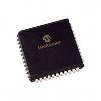
PIC16C774-E/L Microchip Technology, PIC16C774-E/L Datasheet - Page 29

PIC16C774-E/L
Manufacturer Part Number
PIC16C774-E/L
Description
IC MCU OTP 4KX14 A/D PWM 44PLCC
Manufacturer
Microchip Technology
Series
PIC® 16Cr
Datasheets
1.PIC16F616T-ISL.pdf
(8 pages)
2.PIC16C773SO.pdf
(201 pages)
3.PIC16C774P.pdf
(13 pages)
4.PIC16C774P.pdf
(16 pages)
Specifications of PIC16C774-E/L
Core Processor
PIC
Core Size
8-Bit
Speed
20MHz
Connectivity
I²C, SPI, UART/USART
Peripherals
Brown-out Detect/Reset, POR, PWM, WDT
Number Of I /o
33
Program Memory Size
7KB (4K x 14)
Program Memory Type
OTP
Ram Size
256 x 8
Voltage - Supply (vcc/vdd)
4 V ~ 5.5 V
Data Converters
A/D 10x12b
Oscillator Type
External
Operating Temperature
-40°C ~ 125°C
Package / Case
44-PLCC
For Use With
DVA16XL441 - ADAPTER DEVICE ICE 44PLCC
Lead Free Status / RoHS Status
Lead free / RoHS Compliant
Eeprom Size
-
Other names
PIC16C774E/L
Available stocks
Company
Part Number
Manufacturer
Quantity
Price
Company:
Part Number:
PIC16C774-E/L
Manufacturer:
Microchip Technology
Quantity:
10 000
- PIC16F616T-ISL PDF datasheet
- PIC16C773SO PDF datasheet #2
- PIC16C774P PDF datasheet #3
- PIC16C774P PDF datasheet #4
- Current page: 29 of 201
- Download datasheet (3Mb)
3.2
PORTB is an 8-bit wide bi-directional port. The corre-
sponding data direction register is TRISB. Setting a
TRISB bit (=1) will make the corresponding PORTB pin
an input, i.e., put the corresponding output driver in a
hi-impedance mode. Clearing a TRISB bit (=0) will
make the corresponding PORTB pin an output, i.e., put
the contents of the output latch on the selected pin.
EXAMPLE 3-1:
BCF
CLRF
BSF
MOVLW
MOVWF
Each of the PORTB pins has a weak internal pull-up. A
single control bit can turn on all the pull-ups. This is per-
formed by clearing bit RBPU (OPTION_REG<7>). The
weak pull-up is automatically turned off when the port
pin is configured as an output. The pull-ups are dis-
abled on a Power-on Reset.
The RB0 pin is multiplexed with the external interrupt
(RB0/INT).
FIGURE 3-4:
Data bus
WR TRIS
WR Port
RBPU
RB0/INT
1999 Microchip Technology Inc.
Note 1: I/O pins have diode protection to V
(2)
2: To enable weak pull-ups, set the appropriate TRIS bit(s)
STATUS, RP0
PORTB
STATUS, RP0
0xCF
TRISB
PORTB and the TRISB Register
and clear the RBPU bit (OPTION_REG<7>).
BLOCK DIAGRAM OF RB0 PIN
RD TRIS
RD Port
TRIS Latch
Data Latch
INITIALIZING PORTB
D
D
CK
CK
Schmitt Trigger
Buffer
;
; Initialize PORTB by
; clearing output
; data latches
; Select Bank 1
; Value used to
; initialize data
; direction
; Set RB<3:0> as inputs
; RB<5:4> as outputs
; RB<7:6> as inputs
Q
Q
Q
DD
and V
EN
TTL
Input
Buffer
D
SS
Advance Information
.
V
P
RD Port
DD
weak
pull-up
I/O
pin
(1)
The RB1 pin is multiplexed with the SSP module slave
select (RB1/SS).
FIGURE 3-5:
The RB2 pin is multiplexed with analog channel 8
(RB2/AN8).
FIGURE 3-6:
Data bus
Data bus
WR TRIS
WR TRIS
WR Port
WR Port
SS input
To A/D converter
RBPU
RBPU
Note 1: I/O pins have diode protection to V
Note 1: I/O pins have diode protection to V
(2)
(2)
2: To enable weak pull-ups, set the appropriate TRIS bit(s)
2: To enable weak pull-ups, set the appropriate TRIS bit(s)
and clear the RBPU bit (OPTION_REG<7>).
and clear the RBPU bit (OPTION_REG<7>).
RD TRIS
Data Latch
TRIS Latch
D
D
CK
CK
BLOCK DIAGRAM OF RB1/SS
BLOCK DIAGRAM OF
PIN
RB2/AN8 PIN
RD TRIS
RD Port
RD Port
Data Latch
TRIS Latch
D
D
Q
Q
CK
CK
Schmitt Trigger
Buffer
PIC16C77X
Q
Q
Q
Analog
input mode
EN
D
Q
DD
DD
DS30275A-page 29
and V
and V
EN
TTL
Input
Buffer
TTL
Input
Buffer
RD Port
D
SS
SS
.
.
V
V
P
RD Port
P
DD
DD
weak
pull-up
weak
pull-up
I/O
pin
I/O
pin
(1)
(1)
Related parts for PIC16C774-E/L
Image
Part Number
Description
Manufacturer
Datasheet
Request
R

Part Number:
Description:
IC MCU OTP 8KX14 A/D PWM 44PLCC
Manufacturer:
Microchip Technology
Datasheet:

Part Number:
Description:
IC MCU OTP 8KX14 A/D PWM 44PLCC
Manufacturer:
Microchip Technology
Datasheet:

Part Number:
Description:
IC MCU OTP 8KX14 A/D PWM 44TQFP
Manufacturer:
Microchip Technology
Datasheet:

Part Number:
Description:
IC MCU OTP 8KX14 A/D PWM 44-MQFP
Manufacturer:
Microchip Technology
Datasheet:

Part Number:
Description:
IC MCU OTP 8KX14 A/D PWM 40DIP
Manufacturer:
Microchip Technology
Datasheet:

Part Number:
Description:
IC MCU OTP 8KX14 A/D PWM 44PLCC
Manufacturer:
Microchip Technology
Datasheet:

Part Number:
Description:
IC MCU OTP 8KX14 A/D PWM 40DIP
Manufacturer:
Microchip Technology
Datasheet:

Part Number:
Description:
IC MCU OTP 8KX14 A/D PWM 40DIP
Manufacturer:
Microchip Technology
Datasheet:

Part Number:
Description:
IC MCU OTP 8KX14 A/D PWM 40DIP
Manufacturer:
Microchip Technology
Datasheet:

Part Number:
Description:
IC MCU OTP 8KX14 A/D PWM 44PLCC
Manufacturer:
Microchip Technology
Datasheet:

Part Number:
Description:
IC MCU OTP 8KX14 A/D PWM 44PLCC
Manufacturer:
Microchip Technology
Datasheet:

Part Number:
Description:
IC MCU OTP 8KX14 A/D PWM 44-MQFP
Manufacturer:
Microchip Technology
Datasheet:

Part Number:
Description:
IC MCU OTP 8KX14 A/D PWM 40DIP
Manufacturer:
Microchip Technology
Datasheet:

Part Number:
Description:
IC MCU OTP 8KX14 A/D PWM 44-MQFP
Manufacturer:
Microchip Technology
Datasheet:

Part Number:
Description:
IC MCU OTP 8KX14 A/D PWM 40DIP
Manufacturer:
Microchip Technology
Datasheet:


