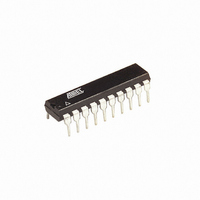
ATTINY26-16PI Atmel, ATTINY26-16PI Datasheet - Page 18

ATTINY26-16PI
Manufacturer Part Number
ATTINY26-16PI
Description
IC AVR MCU 2K 16MHZ IND 20-DIP
Manufacturer
Atmel
Series
AVR® ATtinyr
Specifications of ATTINY26-16PI
Core Processor
AVR
Core Size
8-Bit
Speed
16MHz
Connectivity
USI
Peripherals
Brown-out Detect/Reset, POR, PWM, WDT
Number Of I /o
16
Program Memory Size
2KB (1K x 16)
Program Memory Type
FLASH
Eeprom Size
128 x 8
Ram Size
128 x 8
Voltage - Supply (vcc/vdd)
4.5 V ~ 5.5 V
Data Converters
A/D 11x10b
Oscillator Type
Internal
Operating Temperature
-40°C ~ 85°C
Package / Case
20-DIP (0.300", 7.62mm)
Lead Free Status / RoHS Status
Contains lead / RoHS non-compliant
- Current page: 18 of 182
- Download datasheet (3Mb)
EEPROM Data
Memory
EEPROM Read/Write
Access
EEPROM Address
Register – EEAR
18
ATtiny26(L)
The five different addressing modes for the data memory cover: Direct, Indirect with Displace-
ment, Indirect, Indirect with Pre-decrement, and Indirect with Post-increment. In the Register
File, registers R26 to R31 feature the indirect addressing pointer registers.
The direct addressing reaches the entire data space. The Indirect with Displacement mode fea-
tures a 63 address locations reach from the base address given by the Y- or Z-register.
When using register indirect addressing modes with automatic pre-decrement and post-incre-
ment, the address registers X, Y, and Z are decremented and incremented.
The 32 general purpose working registers, 64 I/O Registers and the 128 bytes of internal data
SRAM in the ATtiny26(L) are all accessible through all these addressing modes.
See “Program and Data Addressing Modes” on page 11 for a detailed description of the different
addressing modes.
The ATtiny26(L) contains 128 bytes of data EEPROM memory. It is organized as a separate
data space, in which single bytes can be read and written (see “Memory Programming” on page
107). The EEPROM has an endurance of at least 100,000 write/erase cycles per location.
The EEPROM Access Registers are accessible in the I/O space.
The write access time is typically 8.3 ms. A self-timing function lets the user software detect
when the next byte can be written. A special EEPROM Ready Interrupt can be set to trigger
when the EEPROM is ready to accept new data.
An ongoing EEPROM write operation will complete even if a reset condition occurs.
In order to prevent unintentional EEPROM writes, a two state write procedure must be followed.
Refer to the description of the EEPROM Control Register for details on this.
When the EEPROM is written, the CPU is halted for two clock cycles before the next instruction
is executed.
When the EEPROM is read, the CPU is halted for four clock cycles before the next instruction is
executed.
• Bit 7 – RES: Reserved Bits
This bit are reserved bit in the ATtiny26(L) and will always read as zero.
• Bit 6..0 – EEAR6..0: EEPROM Address
The EEPROM Address Register – EEAR – specifies the EEPROM address in the 128 bytes
EEPROM space. The EEPROM data bytes are addressed linearly between 0 and 127. The ini-
tial value of EEAR is undefined. A proper value must be written before the EEPROM may be
accessed.
Bit
$1E ($3E)
Read/Write
Initial Value
R
7
–
0
EEAR6
R/W
X
6
EEAR5
R/W
X
5
EEAR4
R/W
X
4
EEAR3
R/W
X
3
EEAR2
R/W
X
2
EEAR1
R/W
X
1
EEAR0
R/W
X
0
EEAR
1477K–AVR–08/10
Related parts for ATTINY26-16PI
Image
Part Number
Description
Manufacturer
Datasheet
Request
R

Part Number:
Description:
Manufacturer:
Atmel Corporation
Datasheet:

Part Number:
Description:
IC AVR MCU 2K 16MHZ IND 32-QFN
Manufacturer:
Atmel
Datasheet:

Part Number:
Description:
IC AVR MCU 2K 16MHZ IND 20-SOIC
Manufacturer:
Atmel
Datasheet:

Part Number:
Description:
IC AVR MCU 2K 16MHZ IND 20-DIP
Manufacturer:
Atmel
Datasheet:

Part Number:
Description:
IC AVR MCU 2K 16MHZ IND 32-QFN
Manufacturer:
Atmel
Datasheet:

Part Number:
Description:
IC AVR MCU 2K 16MHZ COM 20-SOIC
Manufacturer:
Atmel
Datasheet:

Part Number:
Description:
IC AVR MCU 2K 16MHZ IND 20-SOIC
Manufacturer:
Atmel
Datasheet:

Part Number:
Description:
ID MCU AVR 2K 5V 16MHZ 32-QFN
Manufacturer:
Atmel
Datasheet:

Part Number:
Description:
Microcontrollers (MCU) AVR 2K FLASH 128B EE 128B SRAM ADC
Manufacturer:
Atmel
Datasheet:

Part Number:
Description:
IC AVR MCU 2K 16MHZ COM 32-QFN
Manufacturer:
Atmel
Datasheet:

Part Number:
Description:
IC AVR MCU 2K 16MHZ COM 20-DIP
Manufacturer:
Atmel
Datasheet:

Part Number:
Description:
ID MCU AVR 2K 5V 16MHZ 20-DIP
Manufacturer:
Atmel
Datasheet:

Part Number:
Description:
ID MCU AVR 2K 5V 16MHZ 20-SOIC
Manufacturer:
Atmel
Datasheet:

Part Number:
Description:
IC MCU AVR 2K 16MHZ IND 20SOIC
Manufacturer:
Atmel
Datasheet:


