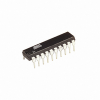
ATTINY26-16PI Atmel, ATTINY26-16PI Datasheet - Page 8

ATTINY26-16PI
Manufacturer Part Number
ATTINY26-16PI
Description
IC AVR MCU 2K 16MHZ IND 20-DIP
Manufacturer
Atmel
Series
AVR® ATtinyr
Specifications of ATTINY26-16PI
Core Processor
AVR
Core Size
8-Bit
Speed
16MHz
Connectivity
USI
Peripherals
Brown-out Detect/Reset, POR, PWM, WDT
Number Of I /o
16
Program Memory Size
2KB (1K x 16)
Program Memory Type
FLASH
Eeprom Size
128 x 8
Ram Size
128 x 8
Voltage - Supply (vcc/vdd)
4.5 V ~ 5.5 V
Data Converters
A/D 11x10b
Oscillator Type
Internal
Operating Temperature
-40°C ~ 85°C
Package / Case
20-DIP (0.300", 7.62mm)
Lead Free Status / RoHS Status
Contains lead / RoHS non-compliant
- Current page: 8 of 182
- Download datasheet (3Mb)
General Purpose
Register File
8
ATtiny26(L)
concept enables instructions to be executed in every clock cycle. The program memory is In-
System programmable Flash memory.
With the relative jump and relative call instructions, the whole address space is directly
accessed. All AVR instructions have a single 16-bit word format, meaning that every program
memory address contains a single 16-bit instruction.
During interrupts and subroutine calls, the return address program counter (PC) is stored on the
Stack. The Stack is effectively allocated in the general data SRAM, and consequently the stack
size is only limited by the total SRAM size and the usage of the SRAM. All user programs must
initialize the SP in the reset routine (before subroutines or interrupts are executed). The 8-bit
Stack Pointer SP is read/write accessible in the I/O space. For programs written in C, the stack
size must be declared in the linker file. Refer to the C user guide for more information.
The 128 bytes data SRAM can be easily accessed through the five different addressing modes
supported in the AVR architecture.
The memory spaces in the AVR architecture are all linear and regular memory maps.
The I/O memory space contains 64 addresses for CPU peripheral functions as Control Regis-
ters, Timer/Counters, and other I/O functions. The memory spaces in the AVR architecture are
all linear and regular memory maps.
A flexible interrupt module has its control registers in the I/O space with an additional Global
Interrupt Enable bit in the Status Register. All the different interrupts have a separate Interrupt
Vector in the Interrupt Vector table at the beginning of the program memory. The different inter-
rupts have priority in accordance with their Interrupt Vector position. The lower the Interrupt
Vector address, the higher the priority.
Figure 3 shows the structure of the 32 general purpose working registers in the CPU.
Figure 3. AVR CPU General Purpose Working Registers
Registers
Purpose
Working
General
7
R13
R14
R15
R16
R17
R26
R27
R28
R29
R30
R31
R0
R1
R2
…
…
0
Addr.
$0D
$0E
$0F
$1A
$1B
$1C
$1D
$1E
$1F
$00
$01
$02
$10
$11
X-register High Byte
Y-register High Byte
Z-register High Byte
X-register Low Byte
Y-register Low Byte
Z-register Low Byte
1477K–AVR–08/10
Related parts for ATTINY26-16PI
Image
Part Number
Description
Manufacturer
Datasheet
Request
R

Part Number:
Description:
Manufacturer:
Atmel Corporation
Datasheet:

Part Number:
Description:
IC AVR MCU 2K 16MHZ IND 32-QFN
Manufacturer:
Atmel
Datasheet:

Part Number:
Description:
IC AVR MCU 2K 16MHZ IND 20-SOIC
Manufacturer:
Atmel
Datasheet:

Part Number:
Description:
IC AVR MCU 2K 16MHZ IND 20-DIP
Manufacturer:
Atmel
Datasheet:

Part Number:
Description:
IC AVR MCU 2K 16MHZ IND 32-QFN
Manufacturer:
Atmel
Datasheet:

Part Number:
Description:
IC AVR MCU 2K 16MHZ COM 20-SOIC
Manufacturer:
Atmel
Datasheet:

Part Number:
Description:
IC AVR MCU 2K 16MHZ IND 20-SOIC
Manufacturer:
Atmel
Datasheet:

Part Number:
Description:
ID MCU AVR 2K 5V 16MHZ 32-QFN
Manufacturer:
Atmel
Datasheet:

Part Number:
Description:
Microcontrollers (MCU) AVR 2K FLASH 128B EE 128B SRAM ADC
Manufacturer:
Atmel
Datasheet:

Part Number:
Description:
IC AVR MCU 2K 16MHZ COM 32-QFN
Manufacturer:
Atmel
Datasheet:

Part Number:
Description:
IC AVR MCU 2K 16MHZ COM 20-DIP
Manufacturer:
Atmel
Datasheet:

Part Number:
Description:
ID MCU AVR 2K 5V 16MHZ 20-DIP
Manufacturer:
Atmel
Datasheet:

Part Number:
Description:
ID MCU AVR 2K 5V 16MHZ 20-SOIC
Manufacturer:
Atmel
Datasheet:

Part Number:
Description:
IC MCU AVR 2K 16MHZ IND 20SOIC
Manufacturer:
Atmel
Datasheet:


