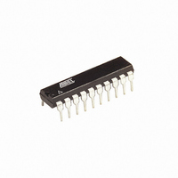
ATTINY26-16PI Atmel, ATTINY26-16PI Datasheet - Page 51

ATTINY26-16PI
Manufacturer Part Number
ATTINY26-16PI
Description
IC AVR MCU 2K 16MHZ IND 20-DIP
Manufacturer
Atmel
Series
AVR® ATtinyr
Specifications of ATTINY26-16PI
Core Processor
AVR
Core Size
8-Bit
Speed
16MHz
Connectivity
USI
Peripherals
Brown-out Detect/Reset, POR, PWM, WDT
Number Of I /o
16
Program Memory Size
2KB (1K x 16)
Program Memory Type
FLASH
Eeprom Size
128 x 8
Ram Size
128 x 8
Voltage - Supply (vcc/vdd)
4.5 V ~ 5.5 V
Data Converters
A/D 11x10b
Oscillator Type
Internal
Operating Temperature
-40°C ~ 85°C
Package / Case
20-DIP (0.300", 7.62mm)
Lead Free Status / RoHS Status
Contains lead / RoHS non-compliant
- Current page: 51 of 182
- Download datasheet (3Mb)
Alternate Functions Of
Port B
1477K–AVR–08/10
Port B has an alternate functions for the ADC, Clocking, Timer/Counters, USI, SPI programming
and pin change interrupt. The ADC is described in “Analog to Digital Converter” on page 94,
Clocking in “AVR CPU Core” on page 7, timers in “Timer/Counters” on page 64 and USI in “Uni-
versal Serial Interface – USI” on page 80. Pin change interrupt triggers on pins PB7 - PB0 if
interrupt is enabled and it is not masked by the alternate functions even if the pin is configured
as an output. See details from “Pin Change Interrupt” on page 62. Pin functions in programming
modes are described in “Memory Programming” on page 107. The alternate functions are shown
in Table 26.
Table 26. Port B Pins Alternate Functions
The alternate pin configuration is as follows:
• ADC10/RESET/PCINT1 – Port B, Bit 7
ADC10: ADC Input Channel 10. Configure the port pins as inputs with the internal pull-ups
switched off to avoid the digital port function from interfering with the function of the analog to
digital converter.
RESET: External Reset input is active low and enabled by unprogramming (“1”) the RSTDISBL
Fuse. Pullup is activated and output driver and digital input are deactivated when the pin is used
as the RESET pin.
PCINT1: Pin Change Interrupt 1 pin. Pin change interrupt is enabled on pin when global interrupt
is enabled, pin change interrupt is enabled and the alternate function do not mask the interrupt.
Port Pin
PB7
PB6
PB5
PB4
PB3
PB2
PB1
PB0
Alternate Functions
ADC10 (ADC Input Channel 10)
RESET (External Reset Input)
PCINT1 (Pin Change Interrupt 1)
ADC9 (ADC Input Channel 9)
INT0 (External Interrupt 0 Input)
T0 (Timer/Counter 0 External Counter Clock Input)
PCINT1 (Pin Change Interrupt 1)
ADC8 (ADC Input Channel 8)
XTAL2 (Crystal Oscillator Output)
PCINT1 (Pin Change Interrupt 1)
ADC7 (ADC Input Channel 7)
XTAL1 (Crystal Oscillator Input)
PCINT1 (Pin Change Interrupt 1)
OC1B (Timer/Counter1 PWM Output B, Timer/Counter1Output Compare B Match
Output)
PCINT0 (Pin Change Interrupt 0)
SCK (USI Clock Input/Output)
SCL (USI External Open-collector Serial Clock)
OC1B (Inverted Timer/Counter1 PWM Output B)
PCINT0 (Pin Change Interrupt 0)
DO (USI Data Output)
OC1A (Timer/Counter1 PWM Output A, Timer/Counter1 Output Compare A Match
Output)
PCINT0 (Pin Change Interrupt 0)
DI (USI Data Input)
SDA (USI Serial Data)
OC1A (Inverted Timer/Counter1 PWM Output A)
PCINT0 (Pin Change Interrupt 0)
51
Related parts for ATTINY26-16PI
Image
Part Number
Description
Manufacturer
Datasheet
Request
R

Part Number:
Description:
Manufacturer:
Atmel Corporation
Datasheet:

Part Number:
Description:
IC AVR MCU 2K 16MHZ IND 32-QFN
Manufacturer:
Atmel
Datasheet:

Part Number:
Description:
IC AVR MCU 2K 16MHZ IND 20-SOIC
Manufacturer:
Atmel
Datasheet:

Part Number:
Description:
IC AVR MCU 2K 16MHZ IND 20-DIP
Manufacturer:
Atmel
Datasheet:

Part Number:
Description:
IC AVR MCU 2K 16MHZ IND 32-QFN
Manufacturer:
Atmel
Datasheet:

Part Number:
Description:
IC AVR MCU 2K 16MHZ COM 20-SOIC
Manufacturer:
Atmel
Datasheet:

Part Number:
Description:
IC AVR MCU 2K 16MHZ IND 20-SOIC
Manufacturer:
Atmel
Datasheet:

Part Number:
Description:
ID MCU AVR 2K 5V 16MHZ 32-QFN
Manufacturer:
Atmel
Datasheet:

Part Number:
Description:
Microcontrollers (MCU) AVR 2K FLASH 128B EE 128B SRAM ADC
Manufacturer:
Atmel
Datasheet:

Part Number:
Description:
IC AVR MCU 2K 16MHZ COM 32-QFN
Manufacturer:
Atmel
Datasheet:

Part Number:
Description:
IC AVR MCU 2K 16MHZ COM 20-DIP
Manufacturer:
Atmel
Datasheet:

Part Number:
Description:
ID MCU AVR 2K 5V 16MHZ 20-DIP
Manufacturer:
Atmel
Datasheet:

Part Number:
Description:
ID MCU AVR 2K 5V 16MHZ 20-SOIC
Manufacturer:
Atmel
Datasheet:

Part Number:
Description:
IC MCU AVR 2K 16MHZ IND 20SOIC
Manufacturer:
Atmel
Datasheet:


