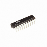
ATTINY26-16PI Atmel, ATTINY26-16PI Datasheet - Page 84

ATTINY26-16PI
Manufacturer Part Number
ATTINY26-16PI
Description
IC AVR MCU 2K 16MHZ IND 20-DIP
Manufacturer
Atmel
Series
AVR® ATtinyr
Specifications of ATTINY26-16PI
Core Processor
AVR
Core Size
8-Bit
Speed
16MHz
Connectivity
USI
Peripherals
Brown-out Detect/Reset, POR, PWM, WDT
Number Of I /o
16
Program Memory Size
2KB (1K x 16)
Program Memory Type
FLASH
Eeprom Size
128 x 8
Ram Size
128 x 8
Voltage - Supply (vcc/vdd)
4.5 V ~ 5.5 V
Data Converters
A/D 11x10b
Oscillator Type
Internal
Operating Temperature
-40°C ~ 85°C
Package / Case
20-DIP (0.300", 7.62mm)
Lead Free Status / RoHS Status
Contains lead / RoHS non-compliant
- Current page: 84 of 182
- Download datasheet (3Mb)
84
ATtiny26(L)
• Bit 3..2 – USICS1..0: Clock Source Select
These bits set the clock source for the Shift Register and counter. The data output latch ensures
that the output is changed at the opposite edge of the sampling of the data input (DI/SDA) when
using external clock source (SCK/SCL). When software strobe or Timer0 overflow clock option is
selected the output latch is transparent and therefore the output is changed immediately. Clear-
ing the USICS1..0 bits enables software strobe option. When using this option, writing a one to
the USICLK bit clocks both the Shift Register and the counter. For external clock source
(USICS1 = 1), the USICLK bit is no longer used as a strobe, but selects between external clock-
ing, and software clocking by the USITC strobe bit.
Table 40 shows the relationship between the USICS1..0 and USICLK setting and clock source
used for the Shift Register and the 4-bit counter.
Table 40. Relations between the USICS1..0 and USICLK Setting
• Bit 1 – USICLK: Clock Strobe
Writing a one to this bit location strobes the Shift Register to shift one step and the counter to
increment by one provided that the USICS1..0 bits are set to zero and by doing so selects the
software clock strobe option. The output will change immediately when the clock strobe is exe-
cuted i.e. in the same instruction cycle. The value shifted into the Shift Register is sampled the
previous instruction cycle. The bit will be read as zero.
When an external clock source is selected (USICS1 = 1), the USICLK function is changed from
a clock strobe to a Clock Select Register. Setting the USICLK bit in this case will select the
USITC strobe bit as clock source for the 4-bit counter (see Table 40).
• Bit 0 – USITC: Toggle Clock Port Pin
Writing a one to this bit location toggles the PORTB2 (SCK/SCL) value from either from 0 to 1, or
1 to 0. The toggling is independent of the DDRB2 setting, but if the PORTB2 value is to be
shown on the pin the DDRB2 must be set as output (to one). This feature allows easy clock gen-
eration when implementing master devices. The bit will be read as zero.
When an external clock source is selected (USICS1 = 1) and the USICLK bit is set to one, writ-
ing to the USITC strobe bit will directly clock the 4-bit counter. This allows an early detection of
when the transfer is done when operating as a master device.
USICS1
0
0
0
1
1
1
1
USICS0
0
0
1
0
1
0
1
USICLK
X
0
1
0
0
1
1
Shift Register Clock
Source
No Clock
Software clock strobe
(USICLK)
Timer/Counter0 overflow
External, positive edge
External, negative edge
External, positive edge
External, negative edge
4-bit Counter Clock
Source
No Clock
Software clock strobe
(USICLK)
Timer/Counter0 overflow
External, both edges
External, both edges
Software clock strobe
(USITC)
Software clock strobe
(USITC)
1477K–AVR–08/10
Related parts for ATTINY26-16PI
Image
Part Number
Description
Manufacturer
Datasheet
Request
R

Part Number:
Description:
Manufacturer:
Atmel Corporation
Datasheet:

Part Number:
Description:
IC AVR MCU 2K 16MHZ IND 32-QFN
Manufacturer:
Atmel
Datasheet:

Part Number:
Description:
IC AVR MCU 2K 16MHZ IND 20-SOIC
Manufacturer:
Atmel
Datasheet:

Part Number:
Description:
IC AVR MCU 2K 16MHZ IND 20-DIP
Manufacturer:
Atmel
Datasheet:

Part Number:
Description:
IC AVR MCU 2K 16MHZ IND 32-QFN
Manufacturer:
Atmel
Datasheet:

Part Number:
Description:
IC AVR MCU 2K 16MHZ COM 20-SOIC
Manufacturer:
Atmel
Datasheet:

Part Number:
Description:
IC AVR MCU 2K 16MHZ IND 20-SOIC
Manufacturer:
Atmel
Datasheet:

Part Number:
Description:
ID MCU AVR 2K 5V 16MHZ 32-QFN
Manufacturer:
Atmel
Datasheet:

Part Number:
Description:
Microcontrollers (MCU) AVR 2K FLASH 128B EE 128B SRAM ADC
Manufacturer:
Atmel
Datasheet:

Part Number:
Description:
IC AVR MCU 2K 16MHZ COM 32-QFN
Manufacturer:
Atmel
Datasheet:

Part Number:
Description:
IC AVR MCU 2K 16MHZ COM 20-DIP
Manufacturer:
Atmel
Datasheet:

Part Number:
Description:
ID MCU AVR 2K 5V 16MHZ 20-DIP
Manufacturer:
Atmel
Datasheet:

Part Number:
Description:
ID MCU AVR 2K 5V 16MHZ 20-SOIC
Manufacturer:
Atmel
Datasheet:

Part Number:
Description:
IC MCU AVR 2K 16MHZ IND 20SOIC
Manufacturer:
Atmel
Datasheet:


