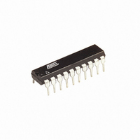
ATTINY26-16PI Atmel, ATTINY26-16PI Datasheet - Page 99

ATTINY26-16PI
Manufacturer Part Number
ATTINY26-16PI
Description
IC AVR MCU 2K 16MHZ IND 20-DIP
Manufacturer
Atmel
Series
AVR® ATtinyr
Specifications of ATTINY26-16PI
Core Processor
AVR
Core Size
8-Bit
Speed
16MHz
Connectivity
USI
Peripherals
Brown-out Detect/Reset, POR, PWM, WDT
Number Of I /o
16
Program Memory Size
2KB (1K x 16)
Program Memory Type
FLASH
Eeprom Size
128 x 8
Ram Size
128 x 8
Voltage - Supply (vcc/vdd)
4.5 V ~ 5.5 V
Data Converters
A/D 11x10b
Oscillator Type
Internal
Operating Temperature
-40°C ~ 85°C
Package / Case
20-DIP (0.300", 7.62mm)
Lead Free Status / RoHS Status
Contains lead / RoHS non-compliant
- Current page: 99 of 182
- Download datasheet (3Mb)
ADC Noise
Canceler Function
ADC Conversion
Result
1477K–AVR–08/10
Special care should be taken when changing differential channels. Once a differential channel
has been selected, the gain stage may take as much as 125 µs to stabilize to the new value.
Thus conversions should not be started within the first 125 µs after selecting a new differential
channel. Alternatively, conversion results obtained within this period should be discarded.
The same settling time should be observed for the first differential conversion after changing
ADC reference (by changing the REFS1:0 bits in ADMUX).
The ADC features a noise canceler that enables conversion during ADC Noise Reduction mode
(see “Power Management and Sleep Modes” on page 37) to reduce noise induced from the
CPU core and other I/O peripherals. If other I/O peripherals must be active during conversion,
this mode works equivalently for Idle mode. To make use of this feature, the following procedure
should be used:
1. Make sure that the ADC is enabled and is not busy converting. Single Conversion mode
2. Enter ADC Noise Reduction mode (or Idle mode). The ADC will start a conversion once
3. If no other interrupts occur before the ADC conversion completes, the ADC interrupt will
After the conversion is complete (ADIF is high), the conversion result can be found in the ADC
Result Registers (ADCL, ADCH).
For single ended conversion, the result is
where V
Table 45 on page 101 and Table 46 on page 102). 0x000 represents analog ground, and 0x3FF
represents the selected reference voltage minus one LSB.
If differential channels are used, the result is
where V
GAIN the selected gain factor, and V
must be higher than V
decoding of the differential input range.
Table 44 shows the resulting output codes if the differential input channel pair (ADCn - ADCm) is
selected with a gain of GAIN and a reference voltage of V
must be selected and the ADC conversion complete interrupt must be enabled.
ADEN = 1
ADSC = 0
ADFR = 0
ADIE = 1
the CPU has been halted.
wake up the CPU and execute the ADC Conversion Complete interrupt routine.
IN
POS
is the voltage on the selected input pin and V
is the voltage on the positive input pin, V
NEG
, otherwise, the ADC value will saturate at 0x000. Figure 56 shows the
ADC
=
(
---------------------------------------------------------------------------
V
POS
ADC
REF
–
the selected voltage reference. Keep in mind that V
V
=
NEG
V
--------------------------
V
IN
REF
V
) GAIN 1024
⋅
REF
⋅
1024
NEG
REF
⋅
REF
the voltage on the negative input pin,
the selected voltage reference (see
.
POS
99
Related parts for ATTINY26-16PI
Image
Part Number
Description
Manufacturer
Datasheet
Request
R

Part Number:
Description:
Manufacturer:
Atmel Corporation
Datasheet:

Part Number:
Description:
IC AVR MCU 2K 16MHZ IND 32-QFN
Manufacturer:
Atmel
Datasheet:

Part Number:
Description:
IC AVR MCU 2K 16MHZ IND 20-SOIC
Manufacturer:
Atmel
Datasheet:

Part Number:
Description:
IC AVR MCU 2K 16MHZ IND 20-DIP
Manufacturer:
Atmel
Datasheet:

Part Number:
Description:
IC AVR MCU 2K 16MHZ IND 32-QFN
Manufacturer:
Atmel
Datasheet:

Part Number:
Description:
IC AVR MCU 2K 16MHZ COM 20-SOIC
Manufacturer:
Atmel
Datasheet:

Part Number:
Description:
IC AVR MCU 2K 16MHZ IND 20-SOIC
Manufacturer:
Atmel
Datasheet:

Part Number:
Description:
ID MCU AVR 2K 5V 16MHZ 32-QFN
Manufacturer:
Atmel
Datasheet:

Part Number:
Description:
Microcontrollers (MCU) AVR 2K FLASH 128B EE 128B SRAM ADC
Manufacturer:
Atmel
Datasheet:

Part Number:
Description:
IC AVR MCU 2K 16MHZ COM 32-QFN
Manufacturer:
Atmel
Datasheet:

Part Number:
Description:
IC AVR MCU 2K 16MHZ COM 20-DIP
Manufacturer:
Atmel
Datasheet:

Part Number:
Description:
ID MCU AVR 2K 5V 16MHZ 20-DIP
Manufacturer:
Atmel
Datasheet:

Part Number:
Description:
ID MCU AVR 2K 5V 16MHZ 20-SOIC
Manufacturer:
Atmel
Datasheet:

Part Number:
Description:
IC MCU AVR 2K 16MHZ IND 20SOIC
Manufacturer:
Atmel
Datasheet:


