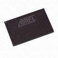
AT91FR40161-CI Atmel, AT91FR40161-CI Datasheet - Page 14

AT91FR40161-CI
Manufacturer Part Number
AT91FR40161-CI
Description
IC MCU ARM7 2M FLASH 120-BGA
Manufacturer
Atmel
Series
AT91SAMr
Datasheet
1.AT91FR40161-CI.pdf
(22 pages)
Specifications of AT91FR40161-CI
Core Processor
ARM7
Core Size
16/32-Bit
Speed
33MHz
Connectivity
EBI/EMI, UART/USART
Peripherals
WDT
Number Of I /o
32
Program Memory Size
2MB (1M x 16)
Program Memory Type
FLASH
Ram Size
136K x 8
Voltage - Supply (vcc/vdd)
2.7 V ~ 3.6 V
Oscillator Type
External
Operating Temperature
-40°C ~ 85°C
Package / Case
120-BGA
Lead Free Status / RoHS Status
Contains lead / RoHS non-compliant
Eeprom Size
-
Data Converters
-
Available stocks
Company
Part Number
Manufacturer
Quantity
Price
Company:
Part Number:
AT91FR40161-CI
Manufacturer:
TI
Quantity:
101
Peripherals
Peripheral Registers
Peripheral Interrupt Control
14
AT94FR40161
Communications can be selected on either COM1 or COM2 and the serial link speed is
limited to 115200 bauds. Because the serial link is the bottleneck in this configuration,
the Flash programming lasts 110 seconds per Mbyte.
Reduced programming time can be achieved by using a faster programming system. An
AT91 Evaluation Board is capable of running a serial link at up to 500 Kbits/sec and can
match the fastest programming allowed by the Flash, for example, about 40 seconds
per Mbyte when the word programming becomes the bottleneck.
The AT91FR40161 peripherals are connected to the 32-bit wide Advanced Peripheral
Bus.
Peripheral registers are only word accessible. Byte and half-word accesses are not sup-
ported. If a byte or a half-word access is attempted, the memory controller automatically
masks the lowest address bits and generates a word access.
Each peripheral has a 16 Kbyte address space allocated (the AIC only has a 4 Kbyte
address space).
The following registers are common to all peripherals:
•
•
•
•
•
Unused bits in the peripheral registers must be written at 0 for upward compatibility.
These bits read 0.
The Interrupt Control of each peripheral is controlled from the status register using the
interrupt mask. The status register bits are ANDed to their corresponding interrupt mask
bits and the result is then ORed to generate the Interrupt Source signal to the Advanced
Interrupt Controller.
The interrupt mask is read in the Interrupt Mask Register and is modified with the Inter-
rupt Enable Register and the Interrupt Disable Register. The enable/disable/status (or
mask) makes it possible to enable or disable peripheral interrupt sources with a non-
interruptible single instruction. This eliminates the need for interrupt masking at the AIC
or core level in real-time and multi-tasking systems.
Control Register – write-only register that triggers a command when a one is written
to the corresponding position at the appropriate address. Writing a zero has no
effect.
Mode Register – read/write register that defines the configuration of the peripheral.
Usually has a value of 0x0 after a reset.
Data Registers – read and/or write register that enables the exchange of data
between the processor and the peripheral.
Status Register – read-only register that returns the status of the peripheral.
Enable/Disable/Status Registers are shadow command registers. Writing a one in
the Enable Register sets the corresponding bit in the Status Register. Writing a one
in the Disable Register resets the corresponding bit and the result can be read in the
Status Register. Writing a bit to zero has no effect. This register access method
maximizes the efficiency of bit manipulation, and enables modification of a register
with a single non-interruptible instruction, replacing the costly read-modify-write
operation.
6040B–ATARM–03/04


