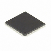
MC68HC16Z1CPV25 Freescale Semiconductor, MC68HC16Z1CPV25 Datasheet - Page 112

MC68HC16Z1CPV25
Manufacturer Part Number
MC68HC16Z1CPV25
Description
IC MPU 1K RAM 25MHZ 144-LQFP
Manufacturer
Freescale Semiconductor
Series
HC16r
Datasheet
1.MC68HC16Z1VEH16.pdf
(500 pages)
Specifications of MC68HC16Z1CPV25
Core Processor
CPU16
Core Size
16-Bit
Speed
25MHz
Connectivity
EBI/EMI, SCI, SPI
Peripherals
POR, PWM, WDT
Number Of I /o
16
Program Memory Type
ROMless
Ram Size
1K x 8
Voltage - Supply (vcc/vdd)
2.7 V ~ 5.5 V
Data Converters
A/D 8x10b
Oscillator Type
Internal
Operating Temperature
-40°C ~ 85°C
Package / Case
144-LQFP
Lead Free Status / RoHS Status
Contains lead / RoHS non-compliant
Eeprom Size
-
Program Memory Size
-
Other names
Q1141110
Available stocks
Company
Part Number
Manufacturer
Quantity
Price
Company:
Part Number:
MC68HC16Z1CPV25
Manufacturer:
MOT
Quantity:
5 510
Company:
Part Number:
MC68HC16Z1CPV25
Manufacturer:
SIEMENS
Quantity:
5 510
Company:
Part Number:
MC68HC16Z1CPV25
Manufacturer:
FREESCAL
Quantity:
624
Company:
Part Number:
MC68HC16Z1CPV25
Manufacturer:
Freescale Semiconductor
Quantity:
10 000
- Current page: 112 of 500
- Download datasheet (6Mb)
5.3.2 Clock Synthesizer Operation
5-6
If a fast or slow reference frequency is provided to the PLL from a source other than a
crystal, or an external system clock signal is applied through the EXTAL pin, the XTAL
pin must be left floating.
either a crystal or an externally supplied reference frequency. A separate power
source increases MCU noise immunity and can be used to run the clock when the
MCU is powered down. A quiet power supply must be used as the V
equate external bypass capacitors should be placed as close as possible to the
V
signal is applied and the PLL is disabled, V
supply.
A voltage controlled oscillator (VCO) in the PLL generates the system clock signal. To
maintain a 50% clock duty cycle, the VCO frequency (f
the system clock frequency, depending on the state of the X bit in SYNCR. The clock
signal is fed back to a divider/counter. The divider controls the frequency of one input
to a phase comparator. The other phase comparator input is a reference signal, either
from the crystal oscillator or from an external source. The comparator generates a con-
trol signal proportional to the difference in phase between the two inputs. This signal
is low-pass filtered and used to correct the VCO output frequency.
Filter circuit implementation can vary, depending upon the external environment and
required clock stability.
works. XFC pin leakage must be kept as low as possible to maintain optimum stability
and PLL performance.
An external filter network connected to the XFC pin is not required when an external
system clock signal is applied and the PLL is disabled (MODCLK = 0 at reset). The
XFC pin must be left floating in this case.
V
DDSYN
DDSYN
pin to assure a stable operating frequency. When an external system clock
is used to power the clock circuits when the system clock is synthesized from
The standard filter used in normal operating environments is a single
0.1 f capacitor, connected from the XFC pin to the V
pin. An alternate filter can be used in high-stability operating environ-
ments to reduce PLL jitter under noisy system conditions. Current
systems that are operating correctly may not require this filter. If the
PLL is not enabled (MODCLK = 0 at reset), the XFC filter is not re-
quired. Versions of the SIM that are configured for either slow or fast
reference use the same filter component values.
Freescale Semiconductor, Inc.
For More Information On This Product,
Figure 5-5
SYSTEM INTEGRATION MODULE
Go to: www.freescale.com
shows two recommended system clock filter net-
NOTE
DDSYN
should be connected to the V
VCO
) is either two or four times
DDSYN
DDSYN
M68HC16 Z SERIES
USER’S MANUAL
supply
source. Ad-
DD
Related parts for MC68HC16Z1CPV25
Image
Part Number
Description
Manufacturer
Datasheet
Request
R
Part Number:
Description:
Manufacturer:
Freescale Semiconductor, Inc
Datasheet:
Part Number:
Description:
Manufacturer:
Freescale Semiconductor, Inc
Datasheet:
Part Number:
Description:
Manufacturer:
Freescale Semiconductor, Inc
Datasheet:
Part Number:
Description:
Manufacturer:
Freescale Semiconductor, Inc
Datasheet:
Part Number:
Description:
Manufacturer:
Freescale Semiconductor, Inc
Datasheet:
Part Number:
Description:
Manufacturer:
Freescale Semiconductor, Inc
Datasheet:
Part Number:
Description:
Manufacturer:
Freescale Semiconductor, Inc
Datasheet:
Part Number:
Description:
Manufacturer:
Freescale Semiconductor, Inc
Datasheet:
Part Number:
Description:
Manufacturer:
Freescale Semiconductor, Inc
Datasheet:
Part Number:
Description:
Manufacturer:
Freescale Semiconductor, Inc
Datasheet:
Part Number:
Description:
Manufacturer:
Freescale Semiconductor, Inc
Datasheet:
Part Number:
Description:
Manufacturer:
Freescale Semiconductor, Inc
Datasheet:
Part Number:
Description:
Manufacturer:
Freescale Semiconductor, Inc
Datasheet:
Part Number:
Description:
Manufacturer:
Freescale Semiconductor, Inc
Datasheet:
Part Number:
Description:
Manufacturer:
Freescale Semiconductor, Inc
Datasheet:


