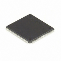
MC68HC16Z1CPV25 Freescale Semiconductor, MC68HC16Z1CPV25 Datasheet - Page 405

MC68HC16Z1CPV25
Manufacturer Part Number
MC68HC16Z1CPV25
Description
IC MPU 1K RAM 25MHZ 144-LQFP
Manufacturer
Freescale Semiconductor
Series
HC16r
Datasheet
1.MC68HC16Z1VEH16.pdf
(500 pages)
Specifications of MC68HC16Z1CPV25
Core Processor
CPU16
Core Size
16-Bit
Speed
25MHz
Connectivity
EBI/EMI, SCI, SPI
Peripherals
POR, PWM, WDT
Number Of I /o
16
Program Memory Type
ROMless
Ram Size
1K x 8
Voltage - Supply (vcc/vdd)
2.7 V ~ 5.5 V
Data Converters
A/D 8x10b
Oscillator Type
Internal
Operating Temperature
-40°C ~ 85°C
Package / Case
144-LQFP
Lead Free Status / RoHS Status
Contains lead / RoHS non-compliant
Eeprom Size
-
Program Memory Size
-
Other names
Q1141110
Available stocks
Company
Part Number
Manufacturer
Quantity
Price
Company:
Part Number:
MC68HC16Z1CPV25
Manufacturer:
MOT
Quantity:
5 510
Company:
Part Number:
MC68HC16Z1CPV25
Manufacturer:
SIEMENS
Quantity:
5 510
Company:
Part Number:
MC68HC16Z1CPV25
Manufacturer:
FREESCAL
Quantity:
624
Company:
Part Number:
MC68HC16Z1CPV25
Manufacturer:
Freescale Semiconductor
Quantity:
10 000
- Current page: 405 of 500
- Download datasheet (6Mb)
PADA[7:0] — Port ADA Data Pins
D.5.4 ADC Control Register 0
ADCTL0 — ADC Control Register 0
RES10 — 10-Bit Resolution
STS[1:0] — Sample Time Selection
PRS[4:0] — Prescaler Rate Selection
M68HC16 Z SERIES
USER’S MANUAL
15
RESET:
A read of PADA[7:0] returns the logic level of the port ADA pins. If an input is not at an
appropriate logic level (that is, outside the defined levels), the read is indeterminate.
Use of a port ADA pin for digital input does not preclude its simultaneous use as an
analog input.
ADCTL0 is used to select 8- or 10-bit conversions, sample time, and ADC clock fre-
quency. Writes to it have immediate effect.
Conversion results are appropriately aligned in result registers to reflect the number of
bits.
Total conversion time is the sum of initial sample time, transfer time, final sample time,
and resolution time. Initial sample time is fixed at two ADC clocks. Transfer time is
fixed at two ADC clocks. Resolution time is fixed at ten ADC clocks for an 8-bit con-
version and twelve ADC clocks for a 10-bit conversion. Final sample time is deter-
mined by the STS[1:0] field. Refer to
The ADC clock is derived from the system clock by a programmable prescaler. ADC
clock period is determined by the value of the PRS field in ADCTL0. The prescaler has
two stages. The first stage is a 5-bit modulus counter. It divides the system clock by
any value from two to 32 (PRS[4:0] = %00000 to %11111). The second stage is a di-
vide-by-two circuit. Refer to
0 = 8-bit conversion
1 = 10-bit conversion
14
13
12
NOT USED
Freescale Semiconductor, Inc.
STS[1:0]
11
For More Information On This Product,
Table D-26 Sample Time Selection
00
01
10
11
10
Table
Go to: www.freescale.com
REGISTER SUMMARY
9
D-27.
Table
8
RES10
16 ADC Clock Periods
2 ADC Clock Periods
4 ADC Clock Periods
8 ADC Clock Periods
7
0
D-26.
Sample Time
6
0
STS[1:0]
5
0
4
0
3
0
PRS[4:0]
2
0
$YFF70A
1
1
D-31
0
1
Related parts for MC68HC16Z1CPV25
Image
Part Number
Description
Manufacturer
Datasheet
Request
R
Part Number:
Description:
Manufacturer:
Freescale Semiconductor, Inc
Datasheet:
Part Number:
Description:
Manufacturer:
Freescale Semiconductor, Inc
Datasheet:
Part Number:
Description:
Manufacturer:
Freescale Semiconductor, Inc
Datasheet:
Part Number:
Description:
Manufacturer:
Freescale Semiconductor, Inc
Datasheet:
Part Number:
Description:
Manufacturer:
Freescale Semiconductor, Inc
Datasheet:
Part Number:
Description:
Manufacturer:
Freescale Semiconductor, Inc
Datasheet:
Part Number:
Description:
Manufacturer:
Freescale Semiconductor, Inc
Datasheet:
Part Number:
Description:
Manufacturer:
Freescale Semiconductor, Inc
Datasheet:
Part Number:
Description:
Manufacturer:
Freescale Semiconductor, Inc
Datasheet:
Part Number:
Description:
Manufacturer:
Freescale Semiconductor, Inc
Datasheet:
Part Number:
Description:
Manufacturer:
Freescale Semiconductor, Inc
Datasheet:
Part Number:
Description:
Manufacturer:
Freescale Semiconductor, Inc
Datasheet:
Part Number:
Description:
Manufacturer:
Freescale Semiconductor, Inc
Datasheet:
Part Number:
Description:
Manufacturer:
Freescale Semiconductor, Inc
Datasheet:
Part Number:
Description:
Manufacturer:
Freescale Semiconductor, Inc
Datasheet:


