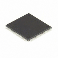
MC68HC16Z1CPV25 Freescale Semiconductor, MC68HC16Z1CPV25 Datasheet - Page 227

MC68HC16Z1CPV25
Manufacturer Part Number
MC68HC16Z1CPV25
Description
IC MPU 1K RAM 25MHZ 144-LQFP
Manufacturer
Freescale Semiconductor
Series
HC16r
Datasheet
1.MC68HC16Z1VEH16.pdf
(500 pages)
Specifications of MC68HC16Z1CPV25
Core Processor
CPU16
Core Size
16-Bit
Speed
25MHz
Connectivity
EBI/EMI, SCI, SPI
Peripherals
POR, PWM, WDT
Number Of I /o
16
Program Memory Type
ROMless
Ram Size
1K x 8
Voltage - Supply (vcc/vdd)
2.7 V ~ 5.5 V
Data Converters
A/D 8x10b
Oscillator Type
Internal
Operating Temperature
-40°C ~ 85°C
Package / Case
144-LQFP
Lead Free Status / RoHS Status
Contains lead / RoHS non-compliant
Eeprom Size
-
Program Memory Size
-
Other names
Q1141110
Available stocks
Company
Part Number
Manufacturer
Quantity
Price
Company:
Part Number:
MC68HC16Z1CPV25
Manufacturer:
MOT
Quantity:
5 510
Company:
Part Number:
MC68HC16Z1CPV25
Manufacturer:
SIEMENS
Quantity:
5 510
Company:
Part Number:
MC68HC16Z1CPV25
Manufacturer:
FREESCAL
Quantity:
624
Company:
Part Number:
MC68HC16Z1CPV25
Manufacturer:
Freescale Semiconductor
Quantity:
10 000
- Current page: 227 of 500
- Download datasheet (6Mb)
M68HC16 Z SERIES
USER’S MANUAL
Data transfer is synchronized with the internally-generated serial clock SCK. Control
bits, CPHA and CPOL, in SPCR0, control clock phase and polarity. Combinations of
CPHA and CPOL determine upon which SCK edge to drive outgoing data from the
MOSI pin and to latch incoming data from the MISO pin.
Baud rate is selected by writing a value from two to 255 into SPBR[7:0] in SPCR0. The
QSPI uses a modulus counter to derive the SCK baud rate from the MCU system
clock.
The following expressions apply to the SCK baud rate:
Giving SPBR[7:0] a value of zero or one disables the baud rate generator and SCK
assumes its inactive state.
The DSCK bit in each command RAM byte inserts either a standard (DSCK = 0) or
user-specified (DSCK = 1) delay from chip-select assertion until the leading edge of
the serial clock. The DSCKL field in SPCR1 determines the length of the user-defined
delay before the assertion of SCK. The following expression determines the actual de-
lay before SCK:
where DSCKL[6:0] equals {1, 2, 3,..., 127}.
When DSCK equals zero, DSCKL[6:0] is not used. Instead, the PCS valid-to-SCK
transition is one-half the SCK period.
There are two transfer length options. The user can choose a default value of eight
bits, or a programmed value from eight to sixteen bits, inclusive. The programmed val-
ue must be written into BITS[3:0] in SPCR0. The BITSE bit in each command RAM
byte determines whether the default value (BITSE = 0) or the BITS[3:0] value (BITSE
= 1) is used.
Table 9-3
Freescale Semiconductor, Inc.
For More Information On This Product,
SPBR[7:0]
shows BITS[3:0] encoding.
PCS to SCK Delay
SCK Baud Rate
QUEUED SERIAL MODULE
Go to: www.freescale.com
=
------------------------------------------------------------------------- -
2 SCK Baud Rate Desired
or
=
------------------------------------ -
2 SPBR[7:0]
=
DSCKL[6:0]
------------------------------ -
f
sys
f
sys
f
sys
9-17
Related parts for MC68HC16Z1CPV25
Image
Part Number
Description
Manufacturer
Datasheet
Request
R
Part Number:
Description:
Manufacturer:
Freescale Semiconductor, Inc
Datasheet:
Part Number:
Description:
Manufacturer:
Freescale Semiconductor, Inc
Datasheet:
Part Number:
Description:
Manufacturer:
Freescale Semiconductor, Inc
Datasheet:
Part Number:
Description:
Manufacturer:
Freescale Semiconductor, Inc
Datasheet:
Part Number:
Description:
Manufacturer:
Freescale Semiconductor, Inc
Datasheet:
Part Number:
Description:
Manufacturer:
Freescale Semiconductor, Inc
Datasheet:
Part Number:
Description:
Manufacturer:
Freescale Semiconductor, Inc
Datasheet:
Part Number:
Description:
Manufacturer:
Freescale Semiconductor, Inc
Datasheet:
Part Number:
Description:
Manufacturer:
Freescale Semiconductor, Inc
Datasheet:
Part Number:
Description:
Manufacturer:
Freescale Semiconductor, Inc
Datasheet:
Part Number:
Description:
Manufacturer:
Freescale Semiconductor, Inc
Datasheet:
Part Number:
Description:
Manufacturer:
Freescale Semiconductor, Inc
Datasheet:
Part Number:
Description:
Manufacturer:
Freescale Semiconductor, Inc
Datasheet:
Part Number:
Description:
Manufacturer:
Freescale Semiconductor, Inc
Datasheet:
Part Number:
Description:
Manufacturer:
Freescale Semiconductor, Inc
Datasheet:


