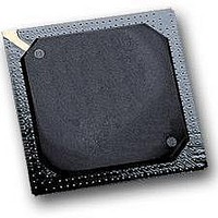
MPC564CVR40 Freescale Semiconductor, MPC564CVR40 Datasheet - Page 791

MPC564CVR40
Manufacturer Part Number
MPC564CVR40
Description
IC MPU 32BIT W/CODE COMP 388PBGA
Manufacturer
Freescale Semiconductor
Series
MPC5xxr
Specifications of MPC564CVR40
Core Processor
PowerPC
Core Size
32-Bit
Speed
40MHz
Connectivity
CAN, EBI/EMI, SCI, SPI, UART/USART
Peripherals
POR, PWM, WDT
Number Of I /o
56
Program Memory Size
512KB (512K x 8)
Program Memory Type
FLASH
Ram Size
32K x 8
Voltage - Supply (vcc/vdd)
2.5 V ~ 2.7 V
Data Converters
A/D 32x10b
Oscillator Type
External
Operating Temperature
-40°C ~ 85°C
Package / Case
388-BGA
Processor Series
MPC5xx
Core
PowerPC
Data Bus Width
32 bit
Data Ram Size
32 KB
Interface Type
CAN, JTAG, QSPI, SCI, SPI, UART
Maximum Clock Frequency
40 MHz
Number Of Programmable I/os
56
Number Of Timers
2
Maximum Operating Temperature
+ 85 C
Mounting Style
SMD/SMT
Minimum Operating Temperature
- 40 C
On-chip Adc
2 (10 bit, 32 Channel)
For Use With
MPC564EVB - KIT EVAL FOR MPC561/562/563/564
Lead Free Status / RoHS Status
Lead free / RoHS Compliant
Eeprom Size
-
Lead Free Status / Rohs Status
Details
Available stocks
Company
Part Number
Manufacturer
Quantity
Price
Company:
Part Number:
MPC564CVR40
Manufacturer:
Freescale Semiconductor
Quantity:
10 000
- Current page: 791 of 1420
- Download datasheet (11Mb)
Freescale Semiconductor
.
Bits
8:15
POL
6:7
0
1
2
3
4
5
0
0
0
1
Control Bits
Name
FREN
TRSP
DDR
POL
EN
PIN
EN
CP
—
0
0
1
0
Pin input status bit — The PIN bit reflects the state present on the MPWMSM signal. The
software can thus monitor the pin state.
The PIN bit is a read-only bit. Writing to the PIN bit has no effect.
Data direction register — The DDR bit indicates the direction for the signal when the PWM
function is not used (disable mode).
0 signal is in input.
1 signal is in output.
The DDR bit is cleared by reset.
Table 17-30
direction register (DDR) bit.
Freeze enable bit — This active high read/write control bit enables the MPWMSM to recognize
the freeze signal on the MIOB.
0 MPWMSM not frozen even if the MIOB freeze line is active.
1 MPWMSM frozen if the MIOB freeze line is active.
The FREN is cleared by reset.
Transparent mode — The TRSP bit indicates that the MPWMSM is in transparent mode. In
transparent mode, when the software writes to either the MPWMPERR or MPWMPULR1 register
the value written is immediately transferred to the counter or register MPWMPULR2 respectively.
0 Double-buffered mode.
1 Transparent mode.
The TRSP bit is cleared by reset.
Output polarity control bit — The POL bit works in conjunction with the EN bit and controls
whether the MPWMSM drives the signal with the direct or the inverted value of the output flip-flop.
Table 17-30
direction register (DDR) bit.
Enable PWM signal generation — The EN bit defines whether the MPWMSM generates a PWM
signal or is used as an I/O channel:
0 PWM generation disabled (signal can be used as I/O).
1 PWM generation enabled (the signal is in output mode).
Each time the submodule is enabled, the value of CP is loaded into the prescaler.
The EN bit is cleared by reset.
Reserved
Clock prescaler — This 8-bit read/write data register stores the modulus value for loading into
the built-in 8-bit clock prescaler. The value loaded defines the divide ratio for the signal that clocks
the MPWMSM. The new value is loaded into the prescaler counter on the prescaler counter
overflow, or upon the EN bit of the MPWMSCR being set.
Table 17-31
DDR
X
0
1
0
Table 17-30. PWMSM Output Signal Polarity Selection
Direction
lists the different uses for the polarity (POL) bit, the enable (EN) bit and the data
lists the different uses for the polarity (POL) bit, the enable (EN) bit and the data
gives the clock divide ratio according to the value of CP.
Table 17-29. MPWMSCR Bit Descriptions
Signal
Output
Output
MPC561/MPC563 Reference Manual, Rev. 1.2
Input
Input
Signal State
Always Low
High Pulse
INPUT
INPUT
Description
Periodic Edge
Falling Edge
—
—
—
Modular Input/Output Subsystem (MIOS14)
Variable Edge
Rising Edge
—
—
—
InterruptIon
Falling Edge
Optional
—
—
—
17-59
Related parts for MPC564CVR40
Image
Part Number
Description
Manufacturer
Datasheet
Request
R

Part Number:
Description:
MPC5 1K0 5%
Manufacturer:
TE Connectivity
Datasheet:

Part Number:
Description:
MPC5 500R 5%
Manufacturer:
TE Connectivity
Datasheet:

Part Number:
Description:
MPC5 5K0 5%
Manufacturer:
Tyco Electronics
Datasheet:

Part Number:
Description:
MPC5 5R0 5%
Manufacturer:
Tyco Electronics
Datasheet:

Part Number:
Description:
MPC5 50K 5%
Manufacturer:
Tyco Electronics
Datasheet:

Part Number:
Description:
MPC5 1R0 5%
Manufacturer:
Tyco Electronics
Datasheet:
Part Number:
Description:
Manufacturer:
Freescale Semiconductor, Inc
Datasheet:
Part Number:
Description:
Manufacturer:
Freescale Semiconductor, Inc
Datasheet:
Part Number:
Description:
Manufacturer:
Freescale Semiconductor, Inc
Datasheet:
Part Number:
Description:
Manufacturer:
Freescale Semiconductor, Inc
Datasheet:
Part Number:
Description:
Manufacturer:
Freescale Semiconductor, Inc
Datasheet:


