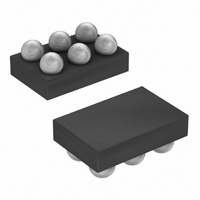
MAX6478BL33AD3+T Maxim Integrated Products, MAX6478BL33AD3+T Datasheet - Page 10

MAX6478BL33AD3+T
Manufacturer Part Number
MAX6478BL33AD3+T
Description
IC LDO REG 300MA 3.3V/ADJ 6-UCSP
Manufacturer
Maxim Integrated Products
Datasheet
1.MAX6469TA15BD3T.pdf
(20 pages)
Specifications of MAX6478BL33AD3+T
Regulator Topology
Positive Fixed or Adjustable
Voltage - Output
3.3V, 1.25 ~ 5.5 V
Voltage - Input
2.5 ~ 5.5 V
Voltage - Dropout (typical)
0.114V @ 300mA, -
Number Of Regulators
1
Current - Output
300mA (Min)
Current - Limit (min)
450mA
Operating Temperature
-40°C ~ 85°C
Mounting Type
Surface Mount
Package / Case
6-UCSP®
Number Of Outputs
1
Polarity
Positive
Input Voltage Max
5.5 V
Output Voltage
1.2 V to 5 V, 3.3 V
Output Type
Adjustable, Fixed
Dropout Voltage (max)
0.032 V at 50 mA
Output Current
0.3 A
Line Regulation
0.09 % / V
Load Regulation
0.2 %
Voltage Regulation Accuracy
1.1 %
Maximum Power Dissipation
840 mW
Maximum Operating Temperature
+ 85 C
Mounting Style
SMD/SMT
Minimum Operating Temperature
- 40 C
Reference Voltage
1.229 V
Lead Free Status / RoHS Status
Lead free / RoHS Compliant
remotely sense the output voltage of the device. Using
FB with an external npn transistor, the current drive capa-
bility can be increased according to the following equa-
tion (Figure 2):
The external npn pass transistor must meet specifica-
tions for current gain, power dissipation, and collector
current. The beta influences the maximum output cur-
rent the circuit can deliver. The largest guaranteed out-
put current is given by I
(min). The transistor’s rated power dissipation must
exceed the actual power dissipated in the transistor.
The power dissipated (PD) equals the maximum load
current (I
put voltage differential: PD = I
V
exceed the maximum load current.
An internal circuit monitors the MAX6469–MAX6484
input and output voltages. When the output voltage is
greater than the input voltage, the internal IN-to-OUT
pass transistor and parasitic diode turn off. An external
voltage applied to OUT does not reverse charge a bat-
tery or power source applied to IN (the leakage path
from OUT to IN is 0.01µA typ). When the output voltage
exceeds the input voltage, OUT powers the device and
shutdown must be logic high (greater than 0.7
RESET asserts until IN exceeds OUT and OUT is above
the specified V
or adjusted regulator OUT nominal voltage).
The MAX6469–MAX6484 maintain a low OUT-to-GND
reverse-current flow when the IN power source is
removed. When IN floats (input battery removed) and
SHDN is pulled up to V
300mA LDO Linear Regulators with Internal
Microprocessor Reset Circuit
Figure 2. High-Current, External Transistor Application
10
OUT
5.0V
MAX6475/MAX6476
MAX6483/MAX6484
______________________________________________________________________________________
). The rated transistor collector current must
GND
IN
LOAD
Reverse Leakage Protection
RESET
OUT
FB
I
Reverse OUT to Ground Current
OUT(TOTAL)
THOUT
(max)) times the maximum input-to-out-
Reverse OUT to IN Current
1A TOTAL CURRENT
threshold (based on the selected
330
OUT
Ω
LOAD
= I
(by an external diode), the
3.3µF
OUT
LOAD
(max) = 300mA × beta
0.1µF
(max) × (V
(β+1)
R
PULLUP
IN
V
CC
µP
= 3.3V
(max) -
V
OUT
).
OUT-to-GND current through the LDO is 40µA (typ). The
regulator output can be held up with an external super
capacitor or backup battery at OUT until the IN battery is
replaced. The RESET output is asserted while the IN bat-
tery is removed to place the system in a low-power
mode. Volatile memory content is maintained until the
super capacitor or battery voltage drops below RAM
standby specifications. RESET deasserts when the IN
battery has been replaced and OUT exceeds the
desired reset threshold. For nonrechargeable backup
battery applications, place a reverse diode between
OUT and the backup battery (to prevent battery charg-
ing). The external diode does not affect the regulator’s
dropout voltage because it is not between the LDO out-
put and the processor/memory V
can be replaced with a current-limiting resistor for
rechargeable backup battery applications.
The MAX6469–MAX6484 include an internal current-
limit circuit that monitors and controls the pass transis-
tor’s gate voltage, limiting the output current to 450mA
(min). The output can be shorted to ground indefinitely
without damaging the part.
When the junction temperature (T
(typ), the thermal sensor signals the shutdown logic,
turning off the pass transistor and allowing the IC to
Figure 3. Battery Backup
LITHIUM ION OR
LITHIUM ION OR
REMOVABLE
REMOVABLE
ALKALINE
ALKALINE
3-CELL
3-CELL
IN
SHDN
IN
SHDN
MAX6469–
MAX6469–
MAX6484
MAX6484
OUT
OUT
SUPERCAP
3.3µF
LITHIUM
3.3µF
3.0V
Thermal Shutdown
CC
Current Limit
J
) exceeds +180°C
supply. The diode
µP
µP
MEMORY
MEMORY


