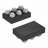
MAX6478BL33AD3+T Maxim Integrated Products, MAX6478BL33AD3+T Datasheet - Page 11

MAX6478BL33AD3+T
Manufacturer Part Number
MAX6478BL33AD3+T
Description
IC LDO REG 300MA 3.3V/ADJ 6-UCSP
Manufacturer
Maxim Integrated Products
Datasheet
1.MAX6469TA15BD3T.pdf
(20 pages)
Specifications of MAX6478BL33AD3+T
Regulator Topology
Positive Fixed or Adjustable
Voltage - Output
3.3V, 1.25 ~ 5.5 V
Voltage - Input
2.5 ~ 5.5 V
Voltage - Dropout (typical)
0.114V @ 300mA, -
Number Of Regulators
1
Current - Output
300mA (Min)
Current - Limit (min)
450mA
Operating Temperature
-40°C ~ 85°C
Mounting Type
Surface Mount
Package / Case
6-UCSP®
Number Of Outputs
1
Polarity
Positive
Input Voltage Max
5.5 V
Output Voltage
1.2 V to 5 V, 3.3 V
Output Type
Adjustable, Fixed
Dropout Voltage (max)
0.032 V at 50 mA
Output Current
0.3 A
Line Regulation
0.09 % / V
Load Regulation
0.2 %
Voltage Regulation Accuracy
1.1 %
Maximum Power Dissipation
840 mW
Maximum Operating Temperature
+ 85 C
Mounting Style
SMD/SMT
Minimum Operating Temperature
- 40 C
Reference Voltage
1.229 V
Lead Free Status / RoHS Status
Lead free / RoHS Compliant
cool. The thermal sensor turns the pass transistor on
again after the IC’s junction temperature cools by 20°C,
resulting in a pulsed output during continuous thermal
overload conditions. Thermal overload protection is
designed to protect the MAX6469–MAX6484 in the
event of fault conditions. For continuous operation, do
not exceed the absolute maximum junction temperature
rating of T
The MAX6469–MAX6484’s maximum power dissipation
depends on the thermal resistance of the case and cir-
cuit board, the temperature difference between the die
junction and the ambient air, and the rate of airflow. The
power dissipation across the device is:
The maximum power dissipation is:
where T
die junction and the surrounding air, Ø
thermal resistance of the package, and Ø
mal resistance through the PC board, copper traces,
and other materials to the surrounding air. The
MAX6469–MAX6476 TDFN package Ø
and the MAX6469–MAX6476 SOT package Ø
110°C/W.
The MAX6469–MAX6484’s ground pin (GND) performs
the dual function of providing an electrical connection
to the system ground and channeling heat away.
Connect GND to the system ground using a large pad
or ground plane. For continuous operation, do not
exceed the absolute maximum junction temperature
rating of T
The MAX6469–MAX6484 feature dual-mode operation:
they operate in either a preset output voltage mode
or an adjustable mode. In preset voltage mode, internal
feedback resistors set the MAX6469–MAX6484’s output
from +1.5V to +3.3V (Table 1). Select this mode by con-
necting SET to ground (MAX6469–MAX6472/
MAX6477–MAX6480). In adjustable mode, select an
output between 1.25V and 5.5V using two external
resistors connected as a voltage-divider to SET (Figure
1). The output voltage is set by the following equation:
where V
J
SET
- T
JMAX
JMAX
A
= 1.23V. To simplify resistor selection:
Operating Region and Power Dissipation
P
MAX
is the temperature difference between the
V
R
= +150°C.
= +150°C.
Applications Information
300mA LDO Linear Regulators with Internal
OUT
1
P = I
= R
______________________________________________________________________________________
= (T
= V
OUT
2
J
Output Voltage Selection
(V
- T
SET
OUT
(V
A
) / (Ø
(1 + R
IN
/ V
- V
SET
JB
OUT
1
+ Ø
/ R
- 1)
)
JB
2
BA
)
JC
(or Ø
BA
)
= 41°C/W,
is the ther-
JC
) is the
Microprocessor Reset Circuit
JC
=
Choose R2 = 50kΩ to maintain stability, accuracy and
high-frequency power-supply rejection. Avoid selecting
resistor values greater than 100kΩ. In preset voltage
mode, the impedance between SET and ground should
always be less than 50kΩ. In most applications, con-
nect SET directly to ground.
MAX6477–MAX6484 UCSP products include internal fil-
tering to yield low output noise without an additional
external bypass capacitor. The devices yield 75µV
(typ) output noise (for V
V
MAX6477–MAX6484 ideal for audio applications.
For stable operation over the full temperature range
and with load currents up to 300mA, use a 3.3µF (min)
ceramic output capacitor with an ESR <0.2Ω. To
reduce noise and improve load transient response, sta-
bility, and power-supply rejection, use large output
capacitor values such as 10µF.
Note that some ceramic capacitors exhibit large capac-
itance and ESR variation with temperature. With capaci-
tor dielectrics such as Z5U and Y5V, use 4.7µF or more
to ensure stability over temperature. With X7R or X5R
capacitor dielectrics, 3.3µF should be sufficient at all
operating temperatures. Higher ESR capacitors require
more capacitance to maintain stability. A graph of the
Region of Stable ESR vs. Load Current is shown in the
Typical Operating Characteristics .
To improve power-supply rejection and transient
response, use a 1µF capacitor between IN and GND.
The MAX6469–MAX6484 remain stable with purely
resistive loads or current loads up to 300mA.
The reset circuit is relatively immune to short-duration,
falling V
Characteristics section shows a graph of the Maximum
Transient Duration vs. Reset Threshold Overdrive for
which reset is not asserted. The graph was produced
using falling V
ing below the reset threshold by the magnitude indicat-
ed (reset threshold overdrive). The graph shows the
maximum pulse width that a falling V
typically have without triggering a reset pulse. As the
amplitude of the transient increases (i.e., goes further
below the reset threshold), the maximum allowable
pulse width decreases. Typically, a V
goes only 10mV below the reset threshold and lasts for
75µs does not trigger a reset pulse.
OUT
= 3.3V). This low-noise feature makes the
OUT
Capacitor Selection and Regulator
OUT
transients. The Typical Operating
transients starting at V
Reset Transient Immunity
OUT
Low-Noise UCSP Output
= 3.0V) and 150µV
OUT
OUT
OUT
transient can
transient that
Stability
and end-
RMS
RMS
(for
11


