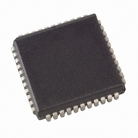
ATMEGA8515L-8JU Atmel, ATMEGA8515L-8JU Datasheet - Page 29

ATMEGA8515L-8JU
Manufacturer Part Number
ATMEGA8515L-8JU
Description
MCU AVR 8K ISP FLASH MEM 44-PLCC
Manufacturer
Atmel
Series
AVR® ATmegar
Specifications of ATMEGA8515L-8JU
Core Processor
AVR
Core Size
8-Bit
Speed
8MHz
Connectivity
EBI/EMI, SPI, UART/USART
Peripherals
Brown-out Detect/Reset, POR, PWM, WDT
Number Of I /o
35
Program Memory Size
8KB (4K x 16)
Program Memory Type
FLASH
Eeprom Size
512 x 8
Ram Size
512 x 8
Voltage - Supply (vcc/vdd)
2.7 V ~ 5.5 V
Oscillator Type
Internal
Operating Temperature
-40°C ~ 85°C
Package / Case
44-LCC (J-Lead)
Processor Series
ATMEGA8x
Core
AVR8
Data Bus Width
8 bit
Data Ram Size
512 B
Interface Type
SPI, USART
Maximum Clock Frequency
8 MHz
Number Of Programmable I/os
35
Number Of Timers
2
Operating Supply Voltage
2.7 V to 5.5 V
Maximum Operating Temperature
+ 85 C
Mounting Style
SMD/SMT
3rd Party Development Tools
EWAVR, EWAVR-BL
Minimum Operating Temperature
- 40 C
Cpu Family
ATmega
Device Core
AVR
Device Core Size
8b
Frequency (max)
8MHz
Total Internal Ram Size
512Byte
# I/os (max)
35
Number Of Timers - General Purpose
2
Operating Supply Voltage (typ)
3.3/5V
Operating Supply Voltage (max)
5.5V
Operating Supply Voltage (min)
2.7V
Instruction Set Architecture
RISC
Operating Temp Range
-40C to 85C
Operating Temperature Classification
Industrial
Mounting
Surface Mount
Pin Count
44
Package Type
PLCC
For Use With
ATSTK600 - DEV KIT FOR AVR/AVR32770-1007 - ISP 4PORT ATMEL AVR MCU SPI/JTAGATAVRISP2 - PROGRAMMER AVR IN SYSTEMATSTK500 - PROGRAMMER AVR STARTER KIT
Lead Free Status / RoHS Status
Lead free / RoHS Compliant
Data Converters
-
Lead Free Status / Rohs Status
Details
Available stocks
Company
Part Number
Manufacturer
Quantity
Price
Part Number:
ATMEGA8515L-8JU
Manufacturer:
ATMEL/爱特梅尔
Quantity:
20 000
XMEM Register
Description
MCU Control Register –
MCUCR
Extended MCU Control
Register – EMCUCR
2512K–AVR–01/10
Figure 16. External Data Memory Cycles with SRWn1 = 1 and SRWn0 = 1
Note:
• Bit 7 – SRE: External SRAM/XMEM Enable
Writing SRE to one enables the External Memory Interface.The pin functions AD7:0,
A15:8, ALE, WR, and RD are activated as the alternate pin functions. The SRE bit over-
rides any pin direction settings in the respective Data Direction Registers. Writing SRE
to zero, disables the External Memory Interface and the normal pin and data direction
settings are used.
• Bit 6 – SRW10: Wait State Select Bit
For a detailed description, see common description for the SRWn bits below (EMCUCR
description).
• Bit 6..4 – SRL2, SRL1, SRL0: Wait State Sector Limit
It is possible to configure different wait states for different external memory addresses.
The External Memory address space can be divided in two sectors that have separate
wait state bits. The SRL2, SRL1, and SRL0 bits select the splitting of these sectors, see
Table 2 and Figure 11. By default, the SRL2, SRL1, and SRL0 bits are set to zero and
the entire External Memory address space is treated as one sector. When the entire
System Clock (CLK
Bit
Read/Write
Initial Value
Bit
Read/Write
Initial Value
DA7:0 (XMBK = 0)
DA7:0 (XMBK = 1)
1. SRWn1 = SRW11 (upper sector) or SRW01 (lower sector), SRWn0 = SRW10 (upper
DA7:0
A15:8
CPU
ALE
WR
RD
sector) or SRW00 (lower sector)
The ALE pulse in period T7 is only present if the next instruction accesses the RAM
(internal or external).
)
Prev. Addr.
Prev. Data
Prev. Data
Prev. Data
SRE
R/W
SM0
R/W
7
0
7
0
T1
SRW10
SRL2
R/W
R/W
6
0
6
0
Address
Address
Address
T2
SRL1
R/W
R/W
SE
XX
5
0
5
0
Address
T3
SRL0
SM1
R/W
R/W
Data
Data
Data
4
0
4
0
SRW01
ISC11
R/W
R/W
T4
3
0
3
0
SRW00
ISC10
R/W
R/W
2
0
2
0
ATmega8515(L)
T5
SRW11
ISC01
R/W
R/W
1
0
1
0
T6
ISC00
ISC2
R/W
R/W
0
0
0
0
(1)
T7
EMCUCR
MCUCR
29


