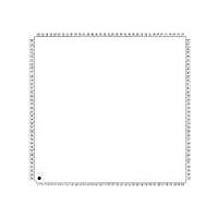
XR17D158CV-F Exar Corporation, XR17D158CV-F Datasheet - Page 22

XR17D158CV-F
Manufacturer Part Number
XR17D158CV-F
Description
IC UART PCI BUS OCTAL 144LQFP
Manufacturer
Exar Corporation
Type
IrDA or RS- 485r
Datasheet
1.XR17D158CV-F.pdf
(73 pages)
Specifications of XR17D158CV-F
Number Of Channels
8
Package / Case
144-LQFP
Features
*
Fifo's
64 Byte
Protocol
RS485
Voltage - Supply
3.3V, 5V
With Auto Flow Control
Yes
With Irda Encoder/decoder
Yes
With False Start Bit Detection
Yes
With Modem Control
Yes
Mounting Type
Surface Mount
Data Rate
6.25 Mbps
Supply Voltage (max)
5.5 V
Supply Voltage (min)
4.5 V
Supply Current
5 mA
Maximum Operating Temperature
+ 70 C
Minimum Operating Temperature
0 C
Mounting Style
SMD/SMT
Operating Supply Voltage
5 V
No. Of Channels
8
Uart Features
Tx/Rx FIFO Counters
Supply Voltage Range
3V To 5.5V
Operating Temperature Range
0°C To +70°C
Digital Ic Case Style
LQFP
No. Of Pins
144
Rohs Compliant
Yes
Lead Free Status / RoHS Status
Lead free / RoHS Compliant
Lead Free Status / RoHS Status
Lead free / RoHS Compliant, Lead free / RoHS Compliant
Other names
1016-1291
Available stocks
Company
Part Number
Manufacturer
Quantity
Price
Company:
Part Number:
XR17D158CV-F
Manufacturer:
Exar Corporation
Quantity:
10 000
Part Number:
XR17D158CV-F
Manufacturer:
EXAR/艾科嘉
Quantity:
20 000
XR17D158
UNIVERSAL (3.3V AND 5V) PCI BUS OCTAL UART
Each UART can be separately enabled to enter Sleep mode through the Sleep register. Sleep mode reduces
power consumption when the system needs to put the UART(s) to idle. All of these conditions must be satisfied
for the D158 to enter sleep mode:
The D158 stops its crystal oscillator to conserve power in the sleep mode. User can check the XTAL2 pin for
no clock output as an indication that the device has entered the sleep mode.
The D158 resumes normal operation by any of the following:
If the D158 is awakened by any one of the above conditions, it will return to the sleep mode automatically after
all interrupting conditions have been serviced and cleared. If the D158 is awakened by the modem inputs, a
read to the MSR is required to reset the modem inputs. In any case, the sleep mode will not be entered while
an interrupt is pending from any channel. The D158 will stay in the sleep mode of operation until it is disabled
by setting Sleep = 0x00. In this case, the octal UART is awaken by any of the UART channel from a receive
data byte or a change on the serial port. The UART is ready after 32 crystal clocks to ensure full functionality.
Also, a special interrupt is generated with an indication of no pending interrupt. Reading INT0 will clear this
special interrupt. Logic 0 (default) is disable and logic 1 is enable to sleep mode.
Important: The XR17D158 is a versatile device designed to operate with different VCC (core power supply)
and VIO (PCI bus I/O power supply). However, the VCC and VIO must be equal (VCC = VIO) for the sleep
mode to reduce power consumption. Any difference in these voltages will result in high currents, when placed
in sleep mode. If sleep mode is used, it is recommended that both VCC and VIO be powered by the PCI bus
VIO power pins. If sleep mode is not used, there is no concern about high currents whether VCC = VIO or VCC
> VIO. In any case, VCC should never be less than VIO.
There are two internal registers that provide device identification and revision, DVID and DREV registers. The
8-bit content in the DVID register provides device identification. A return value of 0x28 from this register
indicates the device is a XR17D158. The DREV register returns an 8-bit value of 0x01 for revision A with 0x02
equals to revision B and so forth. This information is very useful to the software driver for identifying which
device it is communicating with and to keep up with revision changes.
2.2.6
2.2.7
• no interrupts pending (INT0 = 0x00)
• divisor is a non-zero value for all channels (ie. DLL = 0x1)
• sleep mode is enabled (SLEEP = 0xFF)
• modem inputs for all channels are not toggling (MSR bits 0-3 = 0)
• RX input pins for all channels are idling HIGH
• a receive data start bit transition (HIGH to LOW)
• a data byte is loaded to the transmitter, THR or FIFO
• a change of logic state on any of the modem or general purpose serial inputs: CTS#, DSR#, CD#, RI#
SLEEP [31:24] (default 0x00)
Device Identification and Revision
Bit-7 Bit-6 Bit-5 Bit-4 Bit-3 Bit-2 Bit-1 Bit-0
Ch-7
Individual UART Channel Sleep Enable
Ch-6
Ch-5 Ch-4 Ch-3 Ch-2 Ch-1 Ch-0
SLEEP Register
22
xr
REV. 1.2.2


