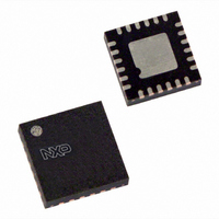
SC16C751BIBS,151 NXP Semiconductors, SC16C751BIBS,151 Datasheet
SC16C751BIBS,151
Specifications of SC16C751BIBS,151
SC16C751BIBS-S
SC16C751BIBS-S


Related parts for SC16C751BIBS,151


SC16C751BIBS,151 Summary of contents
Page 1
SC16C751B 5 V, 3.3 V and 2.5 V UART with 64-byte FIFOs Rev. 02 — 10 October 2008 1. General description The SC16C751B is a Universal Asynchronous Receiver and Transmitter (UART) used for serial data communications. Its principal function is ...
Page 2
... NXP Semiconductors I Standard asynchronous error and framing bits (start, stop, and parity overrun break) I Independent receiver clock input I Transmit, receive, line status, and data set interrupts independently controlled I Fully programmable character formatting: N 5-bit, 6-bit, 7-bit, or 8-bit characters N Even, odd, or no-parity formats ...
Page 3
... NXP Semiconductors 4. Block diagram IOR, IOW RESET INT Fig 1. 5. Pinning information 5.1 Pinning Fig 2. SC16C751B_2 Product data sheet SC16C751B DATA BUS AND CONTROL LOGIC REGISTER SELECT LOGIC INTERRUPT CONTROL LOGIC Block diagram of SC16C751B terminal 1 index area SC16C751BIBS Transparent top view Pin confi ...
Page 4
... NXP Semiconductors 5.2 Pin description Table 2. Symbol CTS INT RESET IOR RTS [ SC16C751B_2 Product data sheet Pin description Pin Type Description 14 I Register select are used during read and write operations to select the UART register to read from or write to Refer to Table 3 12 ...
Page 5
... NXP Semiconductors Table 2. Symbol IOW XTAL1 [2] XTAL2 [1] HVQFN24 package die supply ground is connected to both V be connected to supply ground for proper device operation. For enhanced thermal, electrical, and board level performance, the exposed pad needs to be soldered to the board using a corresponding thermal pad on the board and for proper heat conduction through the board, thermal vias need to be incorporated in the PCB in the thermal pad region ...
Page 6
... NXP Semiconductors status and control registers (IER/ISR), a FIFO Control Register (FCR), line status and control registers (LCR/LSR), modem status and control registers (MCR/MSR), programmable data rate (clock) control registers (DLL/DLM), and a user accessible Scratchpad Register (SPR). Register functions are more fully described in the following paragraphs ...
Page 7
... NXP Semiconductors 6.3 Hardware flow control When automatic hardware flow control is enabled, the SC16C751B monitors the CTS pin for a remote buffer overflow indication and controls the RTS pin for local buffer overflows. Automatic hardware flow control is selected by setting MCR[5] (RTS) and MCR[1] (CTS logic 1. If CTS transitions from a logic logic 1 indicating a fl ...
Page 8
... NXP Semiconductors Fig 3. The generator divides the input 16 clock by any divisor from baud rates can be achieved by selecting the proper divisor values for the MSB and LSB sections of baud rate generator. Programming the baud rate generator registers DLM (MSB) and DLL (LSB) provides a user capability for selecting the desired fi ...
Page 9
... NXP Semiconductors 6.6 Special software initialization sequence Upon reset, the SC16C751B will not be able to receive. A special software initialization sequence must be sent to the device to enable its receiver clock. The following software sequence can be added to the UART initialization routine, and this must be done before other registers are initialized. ...
Page 10
... NXP Semiconductors SC16C751B DATA BUS AND IOR, IOW CONTROL RESET LOGIC REGISTER SELECT CS LOGIC INTERRUPT CONTROL INT LOGIC Fig 4. Internal Loopback mode diagram SC16C751B_2 Product data sheet 5 V, 3.3 V and 2.5 V UART with 64-byte FIFOs TRANSMIT TRANSMIT FIFO SHIFT REGISTERS REGISTER ...
Page 11
... NXP Semiconductors 7. Register descriptions Table 6 assigned bit functions are more fully defined in Table 6. SC16C751B internal registers Register Default [2] General register set RHR THR IER FCR ISR LCR MCR LSR MSR SPR FF [4] Special register set DLL DLM XX [1] The value shown represents the register’s initialized hex value n/a. ...
Page 12
... NXP Semiconductors 7.1 Transmit and Receive Holding Registers (THR and RHR) The serial transmitter section consists of an 8-bit Transmit Hold Register (THR) and Transmit Shift Register (TSR). The status of the THR is provided in the Line Status Register (LSR). Writing to the THR transfers the contents of the data bus (D7 to D0) to the THR, providing that the THR or TSR is empty. The THR empty fl ...
Page 13
... NXP Semiconductors Table 7. Bit Symbol Description 0 IER[0] 7.2.1 IER versus Receive FIFO interrupt mode operation When the receive FIFO (FCR[0] = logic 1), and receive interrupts (IER[0] = logic 1) are enabled, the receive interrupts and register status will reflect the following: • The receive data available interrupts are issued to the external CPU when the FIFO has reached the programmed trigger level ...
Page 14
... NXP Semiconductors 7.3 FIFO Control Register (FCR) This register is used to enable the FIFOs, clear the FIFOs and set the receive FIFO trigger levels. 7.3.1 FIFO mode Table 8. Bit Symbol 7:6 FCR[7] (MSB), FCR[6] (LSB) 5 FCR[5] 4:3 FCR[4:3] 2 FCR[2] 1 FCR[1] 0 FCR[0] Table 9. ...
Page 15
... NXP Semiconductors 7.4 Interrupt Status Register (ISR) The SC16C751B provides four levels of prioritized interrupts to minimize external software interaction. The Interrupt Status Register (ISR) provides the user with four interrupt status bits. Performing a read cycle on the ISR will provide the user with the highest pending interrupt level to be serviced ...
Page 16
... NXP Semiconductors 7.5 Line Control Register (LCR) The Line Control Register is used to specify the asynchronous data communication format. The word length, the number of stop bits, and the parity are selected by writing the appropriate bits in this register. Table 12. Bit 1:0 SC16C751B_2 Product data sheet ...
Page 17
... NXP Semiconductors Table 13. LCR[ Table 14. LCR[ Table 15. LCR[ SC16C751B_2 Product data sheet LCR[5] parity selection LCR[4] LCR[3] Parity selection parity 0 1 odd parity 1 1 even parity 0 1 force parity ‘1’ forced parity ‘0’ LCR[2] stop bit length Word length (bits) ...
Page 18
... NXP Semiconductors 7.6 Modem Control Register (MCR) This register controls the interface with the modem or a peripheral device. Table 16. Bit 3 The flow control can be configured by programming MCR[1] and MCR[5] as shown in Table 17. Table 17. MCR[5] (AFE SC16C751B_2 Product data sheet Modem Control Register bits description ...
Page 19
... NXP Semiconductors 7.7 Line Status Register (LSR) This register provides the status of data transfers between the SC16C751B and the CPU. Table 18. Bit Symbol 7 LSR[7] 6 LSR[6] 5 LSR[5] 4 LSR[4] 3 LSR[3] 2 LSR[2] 1 LSR[1] 0 LSR[0] SC16C751B_2 Product data sheet Line Status Register bits description Description FIFO data error ...
Page 20
... NXP Semiconductors 7.8 Modem Status Register (MSR) This register provides the current state of the control interface signals from the modem, or other peripheral device to which the SC16C751B is connected. Four bits of this register are used to indicate the changed information. These bits are set to a logic 1 whenever a control input from the modem changes state ...
Page 21
... NXP Semiconductors 8. Limiting values Table 22. Limiting values In accordance with the Absolute Maximum Rating System (IEC 60134). Symbol Parameter V supply voltage DD V voltage on any other pin n T ambient temperature amb T storage temperature stg P /pack total power dissipation per package tot 9. Static characteristics Table 23 ...
Page 22
... NXP Semiconductors [1] Except for XTAL2 typically. OL [2] Sleep current might be higher if there is activity on the UART data bus during Sleep mode. 10. Dynamic characteristics Table 24. Dynamic characteristics +85 C; tolerance of V amb Symbol Parameter t pulse width LOW w2 t pulse width HIGH w1 f frequency on pin XTAL1 ...
Page 23
... NXP Semiconductors [1] Applies to external clock, crystal oscillator max 24 MHz. [2] RCLK is an internal signal derived from Divisor Latch LSB (DLL) and Divisor Latch MSB (DLM) divisor latches. [3] Reset pulse must happen when these signals are inactive: CS, IOR, IOW. 10.1 Timing diagrams 6s' ...
Page 24
... NXP Semiconductors active IOW change of state RTS CTS INT IOR Fig 7. Modem input/output timing EXTERNAL CLOCK ------- XTAL1 t w3 Fig 8. External clock timing SC16C751B_2 Product data sheet 5 V, 3.3 V and 2.5 V UART with 64-byte FIFOs t 17d change of state change of state t 18d active ...
Page 25
... NXP Semiconductors RX INT IOR Fig 9. Receive timing TX INT active IOW Fig 10. Transmit timing SC16C751B_2 Product data sheet start bit data bits ( data bits 6 data bits 7 data bits 16 baud rate clock start bit data bits ( data bits 6 data bits 7 data bits active ...
Page 26
... NXP Semiconductors 11. Package outline HVQFN24: plastic thermal enhanced very thin quad flat package; no leads; 24 terminals; body 0.85 mm terminal 1 index area terminal 1 24 index area DIMENSIONS (mm are the original dimensions) (1) A UNIT max. 0.05 0. 0.2 0.00 0.18 Note 1. Plastic or metal protrusions of 0.075 mm maximum per side are not included. ...
Page 27
... NXP Semiconductors 12. Soldering of SMD packages This text provides a very brief insight into a complex technology. A more in-depth account of soldering ICs can be found in Application Note AN10365 “Surface mount reflow soldering description” . 12.1 Introduction to soldering Soldering is one of the most common methods through which packages are attached to Printed Circuit Boards (PCBs), to form electrical circuits ...
Page 28
... NXP Semiconductors 12.4 Reflow soldering Key characteristics in reflow soldering are: • Lead-free versus SnPb soldering; note that a lead-free reflow process usually leads to higher minimum peak temperatures (see reducing the process window • Solder paste printing issues including smearing, release, and adjusting the process window for a mix of large and small components on one board • ...
Page 29
... NXP Semiconductors Fig 12. Temperature profiles for large and small components For further information on temperature profiles, refer to Application Note AN10365 “Surface mount reflow soldering description” . 13. Abbreviations Table 27. Acronym BRG CMOS CPU DLL DLM FIFO LSB MSB TTL UART SC16C751B_2 ...
Page 30
... NXP Semiconductors 14. Revision history Table 28. Revision history Document ID Release date SC16C751B_2 20081010 • Modifications: Section 2 • Section 7.3 “FIFO Control Register mode” • Table 22 “Limiting – symbol V SC16C751B_1 20080424 SC16C751B_2 Product data sheet Data sheet status Product data sheet th “ ...
Page 31
... Right to make changes — NXP Semiconductors reserves the right to make changes to information published in this document, including without limitation specifications and product descriptions, at any time and without notice ...
Page 32
... NXP Semiconductors 17. Contents 1 General description . . . . . . . . . . . . . . . . . . . . . . 1 2 Features . . . . . . . . . . . . . . . . . . . . . . . . . . . . . . . 1 3 Ordering information . . . . . . . . . . . . . . . . . . . . . 2 4 Block diagram . . . . . . . . . . . . . . . . . . . . . . . . . . 3 5 Pinning information . . . . . . . . . . . . . . . . . . . . . . 3 5.1 Pinning . . . . . . . . . . . . . . . . . . . . . . . . . . . . . . . 3 5.2 Pin description . . . . . . . . . . . . . . . . . . . . . . . . . 4 6 Functional description . . . . . . . . . . . . . . . . . . . 5 6.1 Internal registers 6.2 FIFO operation . . . . . . . . . . . . . . . . . . . . . . . . . 6 6.3 Hardware flow control . . . . . . . . . . . . . . . . . . . . 7 6.4 Time-out interrupts . . . . . . . . . . . . . . . . . . . . . . 7 6.5 Programmable baud rate generator . . . . . . . . . 7 6 ...