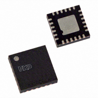
SC16C751BIBS,151 NXP Semiconductors, SC16C751BIBS,151 Datasheet - Page 7

SC16C751BIBS,151
Manufacturer Part Number
SC16C751BIBS,151
Description
IC UART SINGLE W/FIFO 24-HVQFN
Manufacturer
NXP Semiconductors
Datasheet
1.SC16C751BIBS157.pdf
(32 pages)
Specifications of SC16C751BIBS,151
Features
Programmable
Number Of Channels
1, UART
Fifo's
64 Byte
Voltage - Supply
2.5V, 3.3V, 5V
With Auto Flow Control
Yes
With False Start Bit Detection
Yes
With Modem Control
Yes
With Cmos
Yes
Mounting Type
Surface Mount
Package / Case
24-VQFN Exposed Pad, 24-HVQFN, 24-SQFN, 24-DHVQFN
Voltage
2.5 V, 3.3 V, 5 V
Lead Free Status / RoHS Status
Lead free / RoHS Compliant
Other names
935284741151
SC16C751BIBS-S
SC16C751BIBS-S
SC16C751BIBS-S
SC16C751BIBS-S
NXP Semiconductors
SC16C751B_2
Product data sheet
6.3 Hardware flow control
6.4 Time-out interrupts
6.5 Programmable baud rate generator
When automatic hardware flow control is enabled, the SC16C751B monitors the CTS pin
for a remote buffer overflow indication and controls the RTS pin for local buffer overflows.
Automatic hardware flow control is selected by setting MCR[5] (RTS) and MCR[1] (CTS)
to a logic 1. If CTS transitions from a logic 0 to a logic 1 indicating a flow control request,
the SC16C751B will suspend TX transmissions as soon as the stop bit of the character in
process is shifted out. Transmission is resumed after the CTS input returns to a logic 0,
indicating more data may be sent.
With the auto-RTS function enabled, an interrupt is generated when the receive FIFO
reaches the programmed trigger level. The RTS pin will not be forced to a logic 1 (RTS
off), until the receive FIFO reaches the next trigger level. However, the RTS pin will return
to a logic 0 after the data buffer (FIFO) is emptied. However, under the above described
conditions, the SC16C751B will continue to accept data until the receive FIFO is full.
When two interrupt conditions have the same priority, it is important to service these
interrupts correctly. Receive Data Ready and Receive Time Out have the same interrupt
priority (when enabled by IER[0]). The receiver issues an interrupt after the number of
characters have reached the programmed trigger level. In this case, the SC16C751B
FIFO may hold more characters than the programmed trigger level. Following the removal
of a data byte, the user should re-check LSR[0] for additional characters. A Receive Time
Out will not occur if the receive FIFO is empty. The time-out counter is reset at the center
of each stop bit received or each time the receive holding register (RHR) is read. The
actual time-out value is 4 character time.
The SC16C751B supports high speed modem technologies that have increased input
data rates by employing data compression schemes. For example, a 33.6 kbit/s modem
that employs data compression may require a 115.2 kbit/s input data rate. A 128.0 kbit/s
ISDN modem that supports data compression may need an input data rate of 460.8 kbit/s.
A single baud rate generator is provided for the transmitter and receiver, allowing
independent TX/RX channel control. The programmable baud rate generator is capable of
accepting an input clock up to 80 MHz, as required for supporting a 5 Mbit/s data rate.
The SC16C751B can be configured for internal or external clock operation. For internal
clock oscillator operation, an industry standard microprocessor crystal (parallel resonant,
22 pF to 33 pF load) is connected externally between the XTAL1 and XTAL2 pins (see
Figure
internal baud rate generator for standard or custom rates (see
3). Alternatively, an external clock can be connected to the XTAL1 pin to clock the
Rev. 02 — 10 October 2008
5 V, 3.3 V and 2.5 V UART with 64-byte FIFOs
Table
SC16C751B
5).
© NXP B.V. 2008. All rights reserved.
7 of 32


