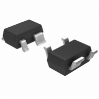
MGA-72543-TR1G Avago Technologies US Inc., MGA-72543-TR1G Datasheet - Page 15

MGA-72543-TR1G
Manufacturer Part Number
MGA-72543-TR1G
Description
IC AMP MMIC LNA GAAS 3V SOT-343
Manufacturer
Avago Technologies US Inc.
Type
General Purpose Amplifierr
Datasheet
1.MGA-72543-TR1G.pdf
(21 pages)
Specifications of MGA-72543-TR1G
Noise Figure
1.42dB
Package / Case
SC-70-4, SC-82-4, SOT-323-4, SOT-343
Current - Supply
60mA ~ 70mA
Frequency
100MHz ~ 6GHz
Gain
13.6dB
P1db
3.2dBm ~ 17.1dBm @ 5mA ~ 60mA
Rf Type
CDMA, TDMA
Test Frequency
2GHz
Voltage - Supply
2.7V ~ 4.2V
Mounting Style
SMD/SMT
Technology
Low Noise Amplifier
Number Of Channels
1
Operating Frequency
6000 MHz
Operating Supply Voltage
3 V
Supply Current
60 mA
Maximum Power Dissipation
250 mW
Maximum Operating Temperature
+ 150 C
Manufacturer's Type
Low Noise Amplifier
Frequency (max)
6GHz
Operating Supply Voltage (min)
2.7V
Operating Supply Voltage (typ)
3V
Operating Supply Voltage (max)
4.2V
Package Type
SOT-343
Mounting
Surface Mount
Pin Count
3 +Tab
Noise Figure (typ)
1.7@6000MHzdB
Lead Free Status / RoHS Status
Lead free / RoHS Compliant
Lead Free Status / RoHS Status
Lead free / RoHS Compliant, Lead free / RoHS Compliant
Other names
516-1829-2
MGA-72543-TR1G
MGA-72543-TR1G
Available stocks
Company
Part Number
Manufacturer
Quantity
Price
Company:
Part Number:
MGA-72543-TR1G
Manufacturer:
AVAGO
Quantity:
201
Company:
Part Number:
MGA-72543-TR1G
Manufacturer:
AVAGO
Quantity:
55 000
Part Number:
MGA-72543-TR1G
Manufacturer:
AVAGO/安华高
Quantity:
20 000
• Adaptive Biasing
For applications in which input power levels vary over a
wide range, it may be useful to dynamically adapt the bias
of the MGA-72543 to match the signal level. This involves
sensing the signal level at some point in the system and
automatically adjusting the bias current of the ampli fier
accordingly. The advantage of adaptive biasing is con-
servation of supply current (longer battery life) by using
only the amount of current necessary to handle the input
signal without distortion.
Adaptive biasing of the MGA-72543 can be accomplished
by either analog or digital means. For the analog control
case, an active current source (discrete device or IC) is
used in lieu of the source bias resistor. For simple digital
control, electronic switches can be used to control the
value of the source resistor in discrete increments. Both
methods of adaptive biasing are depicted in Figure 6.
Figure 6. Adaptive Bias Control.
• Applying the Device Voltage
Common to all methods of biasing, voltage Vd is applied
to the MGA-72543 through the RF Output connection (Pin
2). A RF choke is used to isolate the RF signal from the DC
supply. The bias line is capacitively bypassed to keep RF
from the DC supply lines and prevent resonant dips or
peaks in the response of the amplifier. Where practical, it
may be cost effective to use a length of high impedance
transmission line (preferably O/4) in place of the RFC.
When using the gate bias method, the overall device
voltage is equal to the sum of Vref at Pin 3 and voltage Vd
at Pin 2. As an example, to bias the device at the typical
operating voltage of 3 volts, Vd would be set to 2.5 volts
for a Vref of -0.5 volts. Figure 7 shows a DC schematic of
a gate bias circuit.
Just as for the gate bias method, the overall device
voltage for source resistor biasing is equal to Vref + Vd.
Since Vref is zero when using a source resistor, Vd is the
same as the device operating voltage, typically 3 volts. A
source resistor bias circuit is shown in Figure 8.
15
3
(a) Analog
1
4
2
Control
Analog
(b) Digital
3
1
4
2
Control
Digital
A DC blocking capacitor at the output of the RFIC isolates
the supply voltage from succeeding circuits. If the source
resistor method of biasing is used, the RF input terminal of
the MGA-72543 is at DC ground potential and a blocking
capacitor is not required unless the input is connected di-
rectly to a preceding stage that has a DC voltage present.
Figure 7. DC Schematic for Gate Bias.
Figure 8. DC Schematic of Source Resistor Biasing.
• Biasing for Higher Linearity or Output Power
While the MGA-72543 is designed primarily for use up
to 50 mA in +3 volt applications, the output power can
be increased by using higher currents and/or higher
supply voltages. If higher bias levels are used, appropriate
caution should be observed for both the thermal limits
and the Absolute Maximum Ratings.
As a guideline for operation at higher bias levels, the
Maximum Operating conditions shown in the data sheet
table of Absolute Maximum Ratings should be followed.
This set of conditions is the maximum combination of
bias voltage, bias current, and device temperature that is
recommended for reliable operation. Note: In contrast to
Absolute Maximum ratings, in which exceeding any one
parameter may result in damage to the device, all of the
Maximum Operating conditions may reliably be applied
to the MGA-72543 simultaneously.
Input
Input
RF
RF
Vref = -0.5 V
3
3
1
1
72
72
4
4
R
2
2
bias
RFC
RFC
V
V
d
d
= +2.5 V
Output
Output
= +3 V
RF
RF


