MGA-72543-TR1G Avago Technologies US Inc., MGA-72543-TR1G Datasheet - Page 17
MGA-72543-TR1G
Manufacturer Part Number
MGA-72543-TR1G
Description
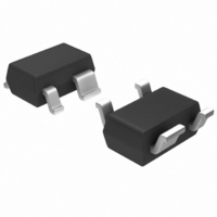
IC AMP MMIC LNA GAAS 3V SOT-343
Manufacturer
Avago Technologies US Inc.
Type
General Purpose Amplifierr
Datasheet
1.MGA-72543-TR1G.pdf
(21 pages)
Specifications of MGA-72543-TR1G
Noise Figure
1.42dB
Package / Case
SC-70-4, SC-82-4, SOT-323-4, SOT-343
Current - Supply
60mA ~ 70mA
Frequency
100MHz ~ 6GHz
Gain
13.6dB
P1db
3.2dBm ~ 17.1dBm @ 5mA ~ 60mA
Rf Type
CDMA, TDMA
Test Frequency
2GHz
Voltage - Supply
2.7V ~ 4.2V
Mounting Style
SMD/SMT
Technology
Low Noise Amplifier
Number Of Channels
1
Operating Frequency
6000 MHz
Operating Supply Voltage
3 V
Supply Current
60 mA
Maximum Power Dissipation
250 mW
Maximum Operating Temperature
+ 150 C
Manufacturer's Type
Low Noise Amplifier
Frequency (max)
6GHz
Operating Supply Voltage (min)
2.7V
Operating Supply Voltage (typ)
3V
Operating Supply Voltage (max)
4.2V
Package Type
SOT-343
Mounting
Surface Mount
Pin Count
3 +Tab
Noise Figure (typ)
1.7@6000MHzdB
Lead Free Status / RoHS Status
Lead free / RoHS Compliant
Lead Free Status / RoHS Status
Lead free / RoHS Compliant, Lead free / RoHS Compliant
Other names
516-1829-2
MGA-72543-TR1G
MGA-72543-TR1G
Available stocks
Company
Part Number
Manufacturer
Quantity
Price
Company:

Part Number:
MGA-72543-TR1G
Manufacturer:
AVAGO
Quantity:
201
Company:
Part Number:
MGA-72543-TR1G
Manufacturer:
AVAGO
Quantity:
55 000
Part Number:
MGA-72543-TR1G
Manufacturer:
AVAGO/安华高
Quantity:
20 000


• Package Footprint
A suggested PCB pad print for the miniature,4-lead SOT-
343 (SC-70) package used by the MGA-72543 is shown in
Figure 10. This pad print provides allowance for package
placement by auto- mated assembly equipment without
adding excessive parasitics that could impair the high
frequency performance of the MGA-72543.The layout is
shown with a footprint of the MGA-72543 superimposed
on the PCB pads for reference.
Figure 10. Recommended PCB Pad Layout for
Avago’s SC70 4L/SOT-343 Products.
• RF bypass
For layouts using the source resistor method of
biasing,both of the ground terminals of the MGA- 72543
must be well bypassed to maintain device stability. Begin-
ning with the package pad print in Figure 10, an RF layout
similar to the one shown in Figure 11 is a good starting
point for using the MGA-72543 with capacitor-bypassed
ground terminals.It is a best practice to use multiple vias
to minimize overall ground path inductance.
Two capacitors are used at each of the PCB pads for
both Pins 1 and 4. The value of the bypass capacitors is
a balance between providing a small reactance for good
RF grounding, yet not being so large that the capacitor’s
parasitics introduce undesirable resonances or loss. If
the source resistor biasing method is used,a ground pad
located near either Pin 1 or 4 pin may be used to connect
the current-setting resistor (Rbias) directly to DC ground.
If the Rbias resistor is not located immediately adjacent
to the MGA-72543 (as may be the case of dynamic control
of the device ’s linearity), then a small series resistor (e.g.,
10Ω) located near the ground terminal will help de-Q the
connection from the MGA-72543 to an external current-
setting circuit.
17
0.031
0.80
0.020
0.50
0.045
1.15
0.051
1.30
0.067
1.71
0.031
.080
• PCB Materials
FR-4 or G-10 type dielectric materials are typical choices
for most low cost wireless applica- tions using single or
multilayer printed circuit boards. The thickness of single-
layer boards usually range from 0.020 to 0.031 inches.
Circuit boards thicker than 0.031 inches are not recom-
mended due to excessive induc- tance in the ground
vias.
Application Example
An example evaluation PCB layout for the MGA-72543 is
shown in Figure 12. This evalua- tion circuit is designed
for operation from a +3-volt supply and includes provision
for a 2-bit DIP switch to set the state of the MGA-72543.
For evaluation purposes, the 2-bit switch is used to set the
device to either of four states: (1)bypass mode – switch
bypasses the amplifier, (2)low noise amplifier mode – low
bias current, (3)and (4) driver ampli- fier modes – high
bias currents.
A completed evaluation amplifier optimized for use at
1900 MHz is shown with all related compo- nents and
SMA connectors in Figure 13. A schematic diagram of the
evaluation circuit is shown in Figure 14 with component
values in Table 1. The on-board resistors R3 and R4 form
the equivalent source bias resistor Rbias as indicated in the
schematic diagram in Figure 14. In this example,resistor
values of R3 = 10Ω and R4 = 24Ω were chosen to set the
nominal device current for the four states to: (1) bypass
mode, 0 mA, (2) LNA mode, 20 mA, (3) driver, 35 mA, and,
(4) driver, 40 mA.
Figure 11. Layout for RF Bypass.
Figure 12. PCB Layout for Evaluation Circuit.
IN
72
MGA-71, MGA-72
Out
HM 8/98
Related parts for MGA-72543-TR1G
Image
Part Number
Description
Manufacturer
Datasheet
Request
R

Part Number:
Description:
IC,Microwave/Millimeter Wave Amplifier,GAAS,SOT-343R,PLASTIC
Manufacturer:
Avago Technologies US Inc.
Datasheet:

Part Number:
Description:
IC AMP MMIC LNA GAAS 3V SOT-343
Manufacturer:
Avago Technologies US Inc.
Datasheet:
Part Number:
Description:
IC AMP MMIC LNA GAAS 3V SOT-343
Manufacturer:
Avago Technologies US Inc.
Datasheet:

Part Number:
Description:
IC,Microwave/Millimeter Wave Amplifier,SINGLE,GAAS,SOT-343R,PLASTIC
Manufacturer:
Avago Technologies US Inc.

Part Number:
Description:
OPTOCOUPLER GATE DRV 2A 16-SOIC
Manufacturer:
Avago Technologies US Inc.
Datasheet:
Part Number:
Description:
OPTOCOUPLER 2CH 2.5A 16-SOIC
Manufacturer:
Avago Technologies US Inc.
Datasheet:

Part Number:
Description:
OPTOCOUPLER GATE DRV 0.4A 16SOIC
Manufacturer:
Avago Technologies US Inc.
Datasheet:

Part Number:
Description:
OPTOCOUPLER 2.0A 250KHZ 8-DIP
Manufacturer:
Avago Technologies US Inc.
Datasheet:

Part Number:
Description:
OPTOCOUPLER 2.0A 250KHZ GW 8-SMD
Manufacturer:
Avago Technologies US Inc.
Datasheet:

Part Number:
Description:
OPTOCOUPLER 2CH 15MBD 3.3V 8SOIC
Manufacturer:
Avago Technologies US Inc.
Datasheet:
Part Number:
Description:
OPTOCOUPLER DARL-OUT 8-DIP
Manufacturer:
Avago Technologies US Inc.
Datasheet:
Part Number:
Description:
OPTOCOUPLER IGBT DRIVE 0.4A 8DIP
Manufacturer:
Avago Technologies US Inc.
Datasheet:
Part Number:
Description:
OPTOCOUPLER DARL-OUT 8-DIP
Manufacturer:
Avago Technologies US Inc.
Datasheet:

Part Number:
Description:
OPTOCOUPLER 1CH 1MBS 8-SMD GW
Manufacturer:
Avago Technologies US Inc.
Datasheet: