MICRF505DEV1 Micrel Inc, MICRF505DEV1 Datasheet - Page 11
MICRF505DEV1
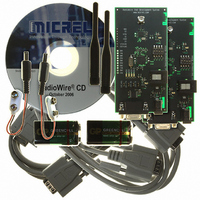
Manufacturer Part Number
MICRF505DEV1
Description
KIT DEV RADIOWIRE 850-950MHZ
Manufacturer
Micrel Inc
Series
RadioWire®r
Type
Transceiver, ISMr
Specifications of MICRF505DEV1
Frequency
850MHz ~ 950MHz
For Use With/related Products
MICRF505
Lead Free Status / RoHS Status
Lead free / RoHS Compliant
Other names
576-1606
Available stocks
Company
Part Number
Manufacturer
Quantity
Price
Company:

Part Number:
MICRF505DEV1
Manufacturer:
Micrel Inc
Quantity:
135


Writing to All Registers
After a power-on, all writable registers should be
written. This is described here.
Writing to all register can be done at any time. To
get the simplest firmware, always write to all
registers. The price to pay for the simplicity is
increased write-time, which leads to increased time
to change the way the MICRF505 works.
What to write
Field
Address:
R/W bit:
Values:
“Address” and “R/W bit” together make 1 octet.
In addition, 22 octets with programming bits are entered.
In total, 23 octets are clocked into the MICRF505.
How to write:
Refer to the figure in the next section, “Writing to n
registers having incremental addresses”.
October 2006
•
•
•
Bring CS high
Use SCLK and IO to clock in the 23 octets
Bring CS low
Comments
‘000000’ (address of the first register to write
to, which is 0)
“0” for writing
1
ControlRegister0. 2
for ControlRegister1 and so on for all of the
octets. So the 22
ControlRegister21. Refer to the specific
sections of this document for actual values.
st
Octet:
Table 4.
wanted
nd
nd
octet wants values for
Octet: wanted values
values
for
11
Writing to n Registers having Incremental
Addresses
In addition to entering all bytes, it is also possible to
enter a set of n bytes, starting from address i = “A6,
A5, … A0”. Typical example: Clock in a new set of
frequency dividers (i.e. change the RF frequency).
“Incremental addresses”. Registers to be written are
located in i, i+1, i+2.
What to write
Field
Address:
R/W bit:
Values:
“Address” and “R/W bit” together make 1 octet.
In addition, n octets with programming bits are entered.
Totally, 1 +n octets are clocked into the MICRF505.
How to write:
In Figure 1, IO is changed at positive edges of SCLK. The
MICRF505 samples the IO line at negative edges. The
value of the R/W bits is always “0” for writing.
CS
SCLK
IO
•
•
•
Bring CS high
Use SCLK and IO to clock in the 1 + n
octets
Bring CS low
A6
register to write to,
Comments
7 bit = A6, A5, …A0 (A6 = msb. A0 = lsb)
(address of first byte to write to)
“0” for writing
n* 8 bits =
D7, D6, …D0 (D7 = msb, D0 = lsb) (written
to control reg. with address ”i”)
D7, D6, …D0 (D7 = msb, D0 = lsb) (written
to control reg. with address ”i+1”)
D7, D6, …D0 (D7 = msb, D0 = lsb) (written
to control reg. with address ”i+n-1”)
Address of first
A5
register i
A0
Figure 2.
Table 5.
RW
RW
D7
Data to write
into register i
Internal load pulse made here
D6
+1 408-944-0800
M9999-103106
Data to write
into register i+1
D2
D1
D0
Related parts for MICRF505DEV1
Image
Part Number
Description
Manufacturer
Datasheet
Request
R

Part Number:
Description:
Manufacturer:
Micrel Inc
Datasheet:
Part Number:
Description:
Manufacturer:
Micrel Inc
Datasheet:
Part Number:
Description:
Manufacturer:
Micrel Inc
Datasheet:
Part Number:
Description:
Manufacturer:
Micrel Inc
Datasheet:
Part Number:
Description:
Manufacturer:
Micrel Inc
Datasheet:
Part Number:
Description:
Manufacturer:
Micrel Inc
Datasheet:
Part Number:
Description:
Manufacturer:
Micrel Inc
Datasheet:
Part Number:
Description:
Manufacturer:
Micrel Inc
Datasheet:
Part Number:
Description:
Manufacturer:
Micrel Inc
Datasheet:
Part Number:
Description:
Manufacturer:
Micrel Inc
Datasheet:
Part Number:
Description:
Manufacturer:
Micrel Inc
Datasheet:
Part Number:
Description:
Manufacturer:
Micrel Inc
Datasheet:
Part Number:
Description:
Manufacturer:
Micrel Inc
Datasheet:
Part Number:
Description:
Manufacturer:
Micrel Inc
Datasheet: