MICRF505DEV1 Micrel Inc, MICRF505DEV1 Datasheet - Page 19
MICRF505DEV1
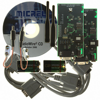
Manufacturer Part Number
MICRF505DEV1
Description
KIT DEV RADIOWIRE 850-950MHZ
Manufacturer
Micrel Inc
Series
RadioWire®r
Type
Transceiver, ISMr
Specifications of MICRF505DEV1
Frequency
850MHz ~ 950MHz
For Use With/related Products
MICRF505
Lead Free Status / RoHS Status
Lead free / RoHS Compliant
Other names
576-1606
Available stocks
Company
Part Number
Manufacturer
Quantity
Price
Company:

Part Number:
MICRF505DEV1
Manufacturer:
Micrel Inc
Quantity:
135


Transceiver Sync/Non-Synchronous Mode
When Sync_en = 1, it will enable the bit
synchronizer in receive mode. The bit synchronizer
clock needs to be programmed, see chapter Bit
synchronizer. The synchronized clock will be set out
on pit DATACLK.
In transmit mode, when Sync_en = 1, the clock
signal on pin DATACLK is a programmed bit rate
clock. Now the transceiver controls the actual data
rate. The data to be transmitted will be sampled on
rising edge of DATACLK. The micro controller can
therefore use the negative edge to change the data
to be transmitted. The clock used for this purpose,
BITRATE_CLK, is programmed in the same way as
the modulator clock and the bit synchronizer clock:
where:
Data Interface
The MICRF505 interface can be divided in to two
separate interfaces, a “programming interface” and a
“Data interface”. The “programming interface” has a
three wire serial programmable interface and is
described in chapter Programming.
The “data interface” can be programmed to sync-
/non-synchronous mode. In synchronous mode the
0000000
0000110
0000111
A6..A0
October 2006
f
BITRATE_CLK
f
control the bit rate, should be equal to the bit
rate (bit rate of 20 kbit/sec requires a clock
requency of 20kHz)
f
Refclk_K: 6 bit divider, values between 1
and 63
BitRate_clkS:
between 0 and 6
BITRATE_CLK
XCO
BitRate_clkS1
: Crystal oscillator frequency
LNA_by
D7
-
: The clock frequency used to
=
BitRate_clkS0
Refclk_K 2
Mod_clkS2
Bit
PA2
D6
rate
f
⋅
XCO
Sync_en
(7-
BitRate_clkS
Mod_clkS1
RefClk_K5
setting,
0
0
1
1
PA1
D5
State
Rx: Bit
synchronization off
Tx: DataClk pin off
Rx: Bit
synchronization on
Tx: DATACLK pin on
)
values
Mod_clkS0
RefClk_K4
PA0
D4
19
BitSync_clkS2
RefClk_K3
Sync_en
MICRF505 is defined as “Master” and provides a
data clock that allows users to utilize low cost micro
controller reference frequency.
The data interface is defined in such a way that all
user actions should take place on falling edge and is
illustrated Figure 9 and 10. The two figures illustrate
the relationship between DATACLK and DATAIXO
in receive mode and transmit mode.
MICRF505 will present data on rising edge and the
“USER” sample data on falling edge in receive
mode.
The User presents data on falling edge and
MICRF505 samples on rising edge in transmit mode.
When entering transmit mode it is important to keep
DATAIXO in tri-state from the time Tx-mode is
entered until user starts sending data. The data is
provided directly to the modulation circuit and
violation of this may/will cause abnormal behavior.
Depending upon the chosen FSK modulation, some
sort of encoding might be needed. The different
modulation types and encoding is described in
chapter Frequency modulation.
Comments
Transparent reception of
data
Transparent transmission
of data
Bit-clock is generated by
transceiver
Bit-clock is generated by
transceiver
D3
DATACLK
DATAIXO
DATACLK
DATAIXO
Figure 11. Data interface in Transmit Mode
Figure 10. Data interface in Receive Mode
BitSync_clkS1
RefClk_K2
Mode1
D2
BitSync_clkS0
RefClk_K1
Mode0
D1
+1 408-944-0800
BitRate_clkS2
M9999-103106
RefClk_K0
Load_en
D0
Related parts for MICRF505DEV1
Image
Part Number
Description
Manufacturer
Datasheet
Request
R

Part Number:
Description:
Manufacturer:
Micrel Inc
Datasheet:
Part Number:
Description:
Manufacturer:
Micrel Inc
Datasheet:
Part Number:
Description:
Manufacturer:
Micrel Inc
Datasheet:
Part Number:
Description:
Manufacturer:
Micrel Inc
Datasheet:
Part Number:
Description:
Manufacturer:
Micrel Inc
Datasheet:
Part Number:
Description:
Manufacturer:
Micrel Inc
Datasheet:
Part Number:
Description:
Manufacturer:
Micrel Inc
Datasheet:
Part Number:
Description:
Manufacturer:
Micrel Inc
Datasheet:
Part Number:
Description:
Manufacturer:
Micrel Inc
Datasheet:
Part Number:
Description:
Manufacturer:
Micrel Inc
Datasheet:
Part Number:
Description:
Manufacturer:
Micrel Inc
Datasheet:
Part Number:
Description:
Manufacturer:
Micrel Inc
Datasheet:
Part Number:
Description:
Manufacturer:
Micrel Inc
Datasheet:
Part Number:
Description:
Manufacturer:
Micrel Inc
Datasheet: